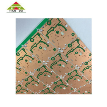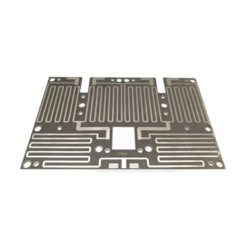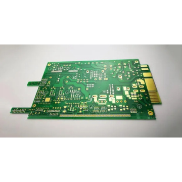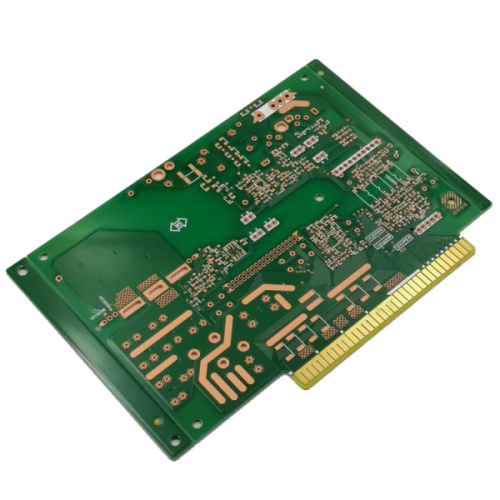

4OZ ~ 6OZ FR4 Aluminum Immersion Gold Multilayer
-
$8.30≥1 Piece/Pieces
- Min. Order:
- 1 Piece/Pieces
- Min. Order:
- 1 Piece/Pieces
Quantity:
Your message must be between 20 to 2000 characters
Contact NowBasic Info
Basic Info
Product Description
Product Description
What is the standard thickness of the copper layer on the PCB?
The general double-sided board is 1oz.
The inner layer of the multilayer board is generally 1/2oz 1/3oz and the outer layer is 1oz 1/2oz 1/3oz.
The copper thickness of the power board is required to be higher, generally 2oz, 3oz and even higher are required.
The thickness and width of the circuit copper in the PCB board are mainly designed according to the current. When the average current of the signal is large, the current that the wiring width can carry should be considered. The relationship between the thickness of the copper foil, the width of the trace and the current in the PCB design .


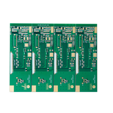
1. Arrange the position of each functional circuit unit according to the circuit flow, so that the layout is convenient for signal circulation, and the signal is kept in the same direction as possible.

3. For circuits operating under the High frequency board, the distribution parameters between components should be considered. Generally, the circuit should be arranged in parallel as much as possible, so that it is not only beautiful, but also PCBA Manufacturing is easy to install and solder, and it is easy to mass produce.