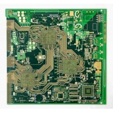


Factory Of Origin High Temperature PCB PCBA
-
$0.10≥1 Piece/Pieces
- Min. Order:
- 1 Piece/Pieces
- Min. Order:
- 1 Piece/Pieces
Your message must be between 20 to 2000 characters
Contact Now
Why copper is used in PCB?
First of all, we need to be clear: the bottom copper plating is beneficial and necessary for the PCB, but the copper plating on the entire board must meet certain conditions.
The benefits of bottom copper plating
1. From the perspective of EMC, the entire surface of the bottom layer is covered with copper, which provides additional shielding protection and noise suppression for the inner and inner signals. At the same time, it also has a certain shielding protection for the underlying equipment and signals.
2. From the perspective of heat dissipation, due to the current increase in PCB board density, BGA main chips also need to consider heat dissipation issues more and more. The entire circuit board is grounded with copper to improve the heat dissipation capacity of the PCB.
3. From a process point of view, the entire board is grounded with copper to make the PCB board evenly distributed.
Although the bottom layer of copper is very suitable for PCB, it still needs to meet some conditions:
1. Through-Hole Assembly should be laid at the same time as much as possible. Don't cover everything at once to avoid the copper skin from cracking, and increase the through-hole on the ground layer of the copper area.
Reason: The copper-clad layer on the surface layer must be broken and destroyed by the components and signal lines on the surface layer.
2. Consider the heat balance of the small package to avoid the monument effect.
Reason: If the entire circuit board is copper-plated, the copper of the component pins will be completely connected to the copper, which will cause the heat to dissipate too fast, which will cause difficulties in desoldering and rework soldering.
3. The grounding of the entire Characteristic impedance PCB is preferably continuous grounding.
Reason: The copper sheet is too close to the ground will change the impedance of the microstrip transmission line, and the discontinuous copper sheet will also have a negative impact on the impedance discontinuity of the transmission line.
4. Some special cases depend on the application scenarios of High frequency board. PCB design should not be an absolute design, but should be weighed and combined with various theories.
Reason: In addition to sensitive signals that need to be grounded, if there are many Microwave radio frequency boards and high frequency mixing pressure plates, a large number of small and long copper breaks will be generated, and the wiring channels are tight. It is necessary to avoid as many copper holes as possible on the surface. To the ground plane. The surface layer can optionally be other than copper.