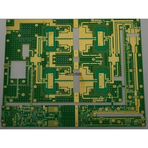
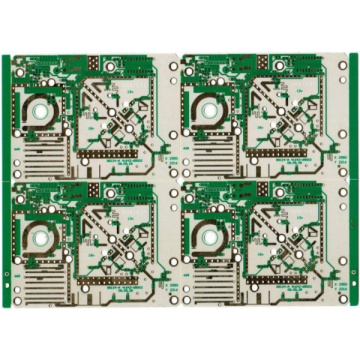
What is HDI PCB?
HDI is an abbreviation for High Density Interconnect. HDI PCB is defined as a circuit board whose wiring density per unit area is higher than that of a traditional circuit board. Compared with traditional PCB technology, they have finer lines and spacing, smaller through holes and capture pads, and higher connection pad density. HDI PCB is used to reduce the size and weight, as well as to enhance the electrical performance of the equipment. HDI PCB is manufactured through microvias and buried vias, and laminated with insulating materials and conductor wiring in order to achieve a higher wiring density mulit-wiring printed board. HDI PCB is the best alternative to high-level and expensive standard laminates or sequential laminates.

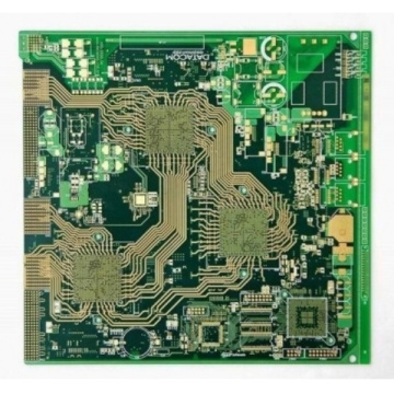
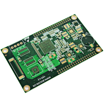
Regarding the electrical requirements of high-speed signals, the PCB must have some AC characteristics, such as the impedance control of the Characteristic impedance PCB, the high frequency transmission capability of the High frequency board and reduce unnecessary radiation. The structure of stripline and microstrip line requires multilayer design. In order to alleviate the quality problems of signal transmission, the Microwave radio frequency board uses insulating materials with low dielectric coefficient and low attenuation ratio. Due to the miniaturization and arraying of electronic components, the density of the PCB must be increased. As a result of ball grid arrays, chip scale packaging, and direct chip attachment assembly methods, PCBs have unprecedented high density. A hole with a diameter less than 150um is called Microvia. It can improve assembly efficiency and space utilization. It is also necessary for the miniaturization of electronic products.

There are many different names for PCBs with this structure. For example, because programming is in a constructive mode of sequence, it is called SBU (Sequence Building Process) in European and American industries. It is called MVP (Microporous Process) in Japanese industry because the pores of such products are much smaller than previous products. It is also called BUM (Building Multilayer Board) because the traditional multilayer is called MLB (Multilayer Board). To avoid confusion, the IPC Printed Circuit Association proposed to name it HDI (High Density Interconnect Technology), but it does not reflect the characteristics of the circuit board. Therefore, most of the PCB industry defines such products as HDI PCB.

HDI PCB has many advantages, such as small size, high speed and high frequency. It is the main component of personal computers, portable computers, mobile phones and personal digital assistants. At present, in addition to mobile phones, HDI PCBs are also widely used in various other consumer products, such as game consoles and MP3s. In addition, since 2006, the application of HDI PCB in notebook computers is expected to become a trend.