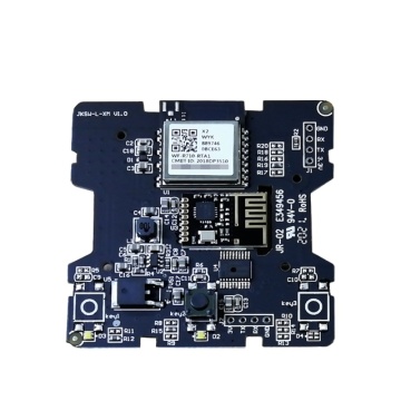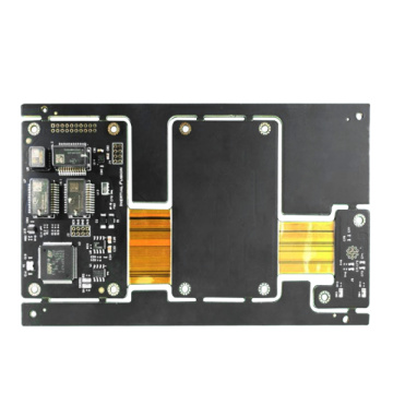


HDI with resin filling counterbore printed circuit board
-
$0.99≥1 Piece/Pieces
- Min. Order:
- 1 Piece/Pieces
- Min. Order:
- 1 Piece/Pieces
Your message must be between 20 to 2000 characters
Contact Now
What is the difference between a blind and buried via?
Blind via: The abbreviation for blind via is Blind via, which connects the outermost layer of the printed circuit board (PCB) with the adjacent inner layer with electroplated holes. Because the opposite side cannot be seen, it is called blind communication. In order to improve the utilization of the space between the plates, blind holes are used.
Blind via holes are through holes on the surface of the PCB. The blind holes are located on the upper and lower layers of the blind via hole PCB, and have a relative height. Used to connect the surface circuit and the lower internal circuit, the depth of the hole usually has a specified ratio (the diameter of the hole). Special attention should be paid to this production method. The drilling depth must be appropriate, otherwise, plating in the hole will be difficult. Therefore, very few processing plants will choose this type of printing method. In fact, it is also possible to drill holes on certain circuit layers that must be connected first, and finally glue them together. A more precise positioning and alignment device must be used.
Buried via: The abbreviation for buried via is Buried via, which refers to the connection between any circuit layers inside a printed circuit board (PCB), but is not connected to the outer layer, that is, there is no through hole extending to the surface of the circuit board. The buried PCB production process cannot be achieved by bonding the circuit board and then drilling it. The drilling operation must be performed on the individual circuit layers. First, the inner layer is partially bonded, then electroplated, and finally fully bonded. Because the operation process is more laborious than the original through holes and blind holes, the price is also the most expensive. This process is usually used for HDI PCB to increase the space utilization rate of other circuit layers.