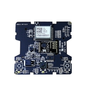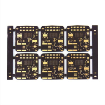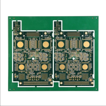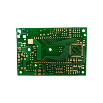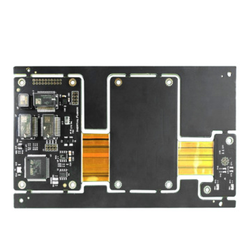
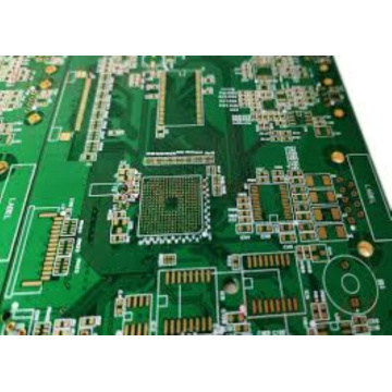
Multilayer PCB with Blind and Buried Hole
-
$0.99≥1 Piece/Pieces
- Min. Order:
- 1 Piece/Pieces
- Min. Order:
- 1 Piece/Pieces
- Transportation:
- Ocean, Land, Air, Express, Others
Quantity:
Your message must be between 20 to 2000 characters
Contact NowBasic Info
Basic Info
| Payment Type: | T/T,Paypal |
|---|---|
| Incoterm: | FOB,EXW |
| Transportation: | Ocean,Land,Air,Express,Others |
Product Description
Product Description
What are blind vias and buried vias?
Blind via: The abbreviation of blind via is Blind via, which connects the outermost layer of the printed circuit board (PCB) with the adjacent inner layers with plated holes. Because the opposite side is invisible, it is called blind pass. In order to improve the utilization of the space between the boards, blind holes are used.

Blind vias are through holes on the surface of the pcb circuit board. The blind holes are arranged on the upper and lower layers of the pcb circuit board, and have relative heights. For connecting surface circuits and lower internal circuits, the depth of the hole usually has a specified ratio (diameter of the hole). Special attention should be paid to this production method. The drilling depth must be appropriate, otherwise, in-hole plating will be difficult. Therefore, very few processors will choose this type of printing method. In fact, it is also possible to preferentially drill holes on some circuit layers that must be connected, and finally glue them together. More precise positioning and alignment devices must be used.


Related Keywords
Related Keywords
You May Also Like
You May Also Like