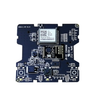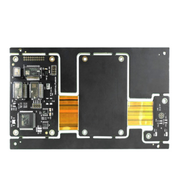


Hdi Buried Blind Via Bga Impedance multilayer pcb
-
$120.00≥1 Piece/Pieces
- Min. Order:
- 1 Piece/Pieces
- Min. Order:
- 1 Piece/Pieces
Your message must be between 20 to 2000 characters
Contact Now
What is HDI stackup?
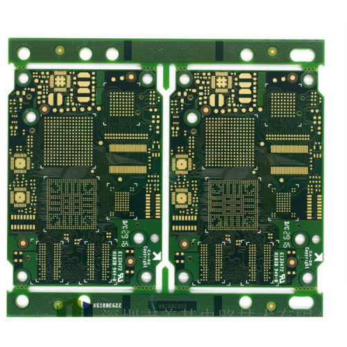
HDI PCB stacking is the use of HDI PCB stacking and wiring in High Quality Prototype PCB Fabrication, which is generally between 8 and 24 layers. The exact number of layers depends on the required trace density, the total number of HDI networks, and the approximate space they will occupy on the PCB.
With such high net counts in HDI PCBs, how to determine the number of layers required in HDI PCB stacks? Assuming that the time-tested HDI manufacturing process is used, it is necessary to estimate how many traces can be accommodated in each layer of board size, and then add other layers for the power and ground planes. For the 1000 net boards mentioned above, we use 10-layer boards as the initial estimate for HDI PCB stackup. Assuming there are 10 layers in total, the thickness of each layer can be calculated and used to determine the trace width required to control the impedance.
Surface-Mount (SMT) & BGA Assembly fine pitch BGA is one of the reasons why some designers are forced to work under the HDI system. The dog-bone sector strategy on the surface is suitable for medium pitch BGA. For differential pairs, it is also necessary to maintain trace coupling under the BGA package.
As with any other design, before creating an HDI PCB stack or starting layout, you should contact the manufacturer to ensure that its DFM guidelines are followed. There are many PCB manufacturers who are highly focused on SMT&Through-Hole Assembly of HDI PCB. They can accommodate very thin and very dense traces, which can accommodate a very large number of layers. Carrying out this important work first can lower cost pcb manufacturing and ensure better yields.