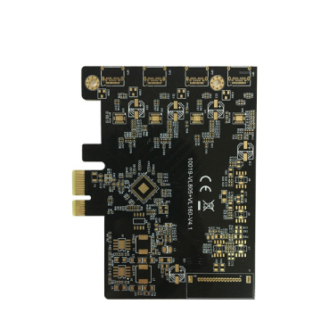
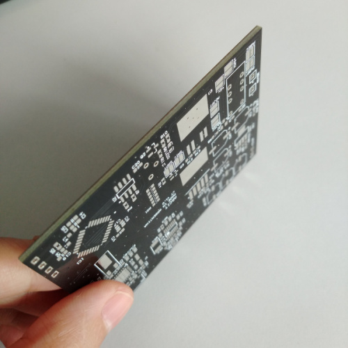
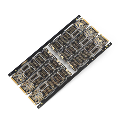
Multilayer PCB Blind and Buried Hole Capability
-
$0.02≥1 Piece/Pieces
- Min. Order:
- 1 Piece/Pieces
- Min. Order:
- 1 Piece/Pieces
Quantity:
Your message must be between 20 to 2000 characters
Contact NowBasic Info
Basic Info
Product Description
Product Description
What is PCB layer stacking?
Printed circuit boards (PCB) are used in various industries. Their construction depends on these industries and applications. Sometimes a single-layer PCB is sufficient, and most of the time, multiple layers are required to support the functionality of the application. During the manufacturing process of custom pcb fabrication, a specific process is performed to ensure its optimal function. When designing the PCB layer, several layers of products and components must be realized and executed.

It is very important to understand and distinguish the various layers of the PCB. In order to better understand the exact thickness of the PCB, subtle distinctions are required to ensure that the PCB works with maximum efficiency. The following layers can usually be seen in a stacked PCB. These may vary, depending on the number of layers, the designer and the design itself.
1. Mechanical layer
This is the basic layer of the PCB. It is used as the outline of the circuit board. This is the basic physical framework of the PCB. This layer also enables designers to communicate the exact location of drill holes and cuts.
2. Retention layer
This layer is similar to the mechanical layer because it can also be used as an outline. However, the function of the holding layer is to define the periphery for placing electrical components, circuit traces, etc. No components or circuits can be placed outside this boundary. This layer limits the routing of CAD tools on specific areas.
1. Routing layer
The routing layer is used to connect components. These layers can be located on both sides of the circuit board. The placement of the layers is up to the designer, who makes decisions based on the application and the components used.
2. Ground plane and power plane
These layers are essential to the normal operation of the PCB. The ground plane is grounded, and the ground is distributed to the entire circuit board and Electronic Components, Electronic connectors and other components.

1. Split the plane
The split plane is basically a split power plane. For example, the power plane on the board can be divided into two. One half of the power plane can be connected to +4 V, and the other half can be connected to -4V. Therefore, components on a board can work with two different voltages depending on their connection.
2. Cover/silk screen layer
The silk screen layer is used to implement text marking for components placed on top of the circuit board. The cover layer performs the same work, except for the bottom of the board. These layers facilitate the manufacturing and debugging process.
1. Solder mask
The copper traces and vias on the circuit board are sometimes covered by a protective layer called a solder mask. This layer keeps dust, dust, humidity and other environmental factors away from the circuit board.
2. Solder paste layer
In PCB assembly, solder paste is used after surface mounting of components. It helps to solder the components to the circuit board. It also helps the solder to flow freely in the PCB composed of surface mount components.


Related Keywords
Related Keywords
Blind and Buried Hole Circuit Board , 5.0mm Board Thickness Circuit Boards , Multi Layer Flexible Pcb
Blind and Buried Hole Circuit Board , 5.0mm Board Thickness Circuit Boards , Multi Layer Flexible Pcb