
DDR4 UDIMM Memory Module Specifications
- Transportation:
- Ocean, Land, Air, Express
Your message must be between 20 to 2000 characters
Contact Now| Payment Type: | T/T,Paypal |
|---|---|
| Incoterm: | FOB,CIF,EXW |
| Transportation: | Ocean,Land,Air,Express |
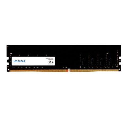
8GB 2666MHz 288-Pin DDR4 UDIMM
Revision History
|
Revision No. |
History |
Draft Date |
Remark |
|
1.0 |
Initial Release |
Apr. 2022 |
|
Ordering Information Table
|
Model |
Density |
Speed |
Organization |
Component Composition |
|
NS08GU4E8 |
8GB |
2666MHz |
1Gx64bit |
DDR4 1Gx8 *8 |
Description
Hengstar Unbuffered DDR4 SDRAM DIMMs (Unbuffered Double Data Rate Synchronous DRAM Dual In-Line Memory Modules) are low power, high-speed operation memory modules that use DDR4 SDRAM devices. NS08GU4E8 is a 1G x 64-bit one rank 8GB DDR4-2666 CL19 1.2V SDRAM Unbuffered DIMM product, based on eight 1G x 8-bit FBGA components. The SPD is programmed to JEDEC standard latency DDR4-2666 timing of 19-19-19 at 1.2V. Each 288-pin DIMM uses gold contact fingers. The SDRAM Unbuffered DIMM is intended for use as main memory when installed in systems such as PCs and workstations.
Features
Power Supply: VDD=1.2V (1.14V to 1.26V)
VDDQ = 1.2V (1.14V to 1.26V)
VPP - 2.5V (2.375V to 2.75V)
VDDSPD=2.25V to 3.6V
Nominal and dynamic on-die termination (ODT) for data, strobe, and mask signals
Low-power auto self refresh (LPASR)
Data bus inversion (DBI) for data bus
On-die VREFDQ generation and calibration
On-board I2C serial presence-detect (SPD) EEPROM
16 internal banks; 4 groups of 4 banks each
Fixed burst chop (BC) of 4 and burst length (BL) of 8 via the mode register set (MRS)
Selectable BC4 or BL8 on-the-fly (OTF)
Databus write cyclic redundancy check (CRC)
Temperature controlled refresh (TCR)
Command/Address (CA) parity
Per DRAM Addressability is supported
8 bit pre-fetch
Fly-by topology
Command/Address latency (CAL)
Terminated control command and address bus
PCB: Height 1.23” (31.25mm)
Gold edge contacts
RoHS Compliant and Halogen-Free
Key Timing Parameters
|
MT/s |
tCK |
CAS Latency |
tRCD |
tRP |
tRAS |
tRC |
CL-tRCD-tRP |
|
DDR4-2666 |
0.75 |
19 |
14.25 |
14.25 |
32 |
46.25 |
19-19-19 |
Address Table
|
Configuration |
Number of |
Bank Group |
Bank |
Row Address |
Column |
Page size |
|
8GB(1Rx8) |
4 |
BG0-BG1 |
BA0-BA1 |
A0-A15 |
A0-A9 |
1 KB |
Functional Block Diagram
8GB, 1Gx64 Module (1Rank of x8)

Absolute Maximum Ratings
Absolute Maximum DC Ratings
|
Symbol |
Parameter |
Rating |
Units |
NOTE |
|
VDD |
Voltage on VDD pin relative to VSS |
-0.3 ~ 1.5 |
V |
1,3 |
|
VDDQ |
Voltage on VDDQ pin relative to VSS |
-0.3 ~ 1.5 |
V |
1,3 |
|
VPP |
Voltage on VPP pin relative to VSS |
-0.3 ~ 3.0 |
V |
4 |
|
VIN, VOUT |
Voltage on any pin except VREFCA relative to VSS |
-0.3 ~ 1.5 |
V |
1,3,5 |
|
TSTG |
Storage Temperature |
-55 to +100 |
°C |
1,2 |
DRAM Component Operating Temperature Range
|
Symbol |
Parameter |
Rating |
Units |
Notes |
|
TOPER |
Normal Operating Temperature Range |
0 to 85 |
°C |
1,2 |
|
Extended Temperature Range |
85 to 95 |
°C |
1,3 |
AC & DC Operating Conditions
Recommended DC Operating Conditions
|
Symbol |
Parameter |
Rating |
Unit |
NOTE |
||
|
Min. |
Typ. |
Max. |
||||
|
VDD |
Supply Voltage |
1.14 |
1.2 |
1.26 |
V |
1,2,3 |
|
VDDQ |
Supply Voltage for Output |
1.14 |
1.2 |
1.26 |
V |
|
|
VPP |
Supply Voltage for DRAM Activating |
2.375 |
2.5 |
2.75 |
V |
3 |
Module Dimensions
Front view

Back view