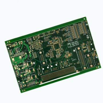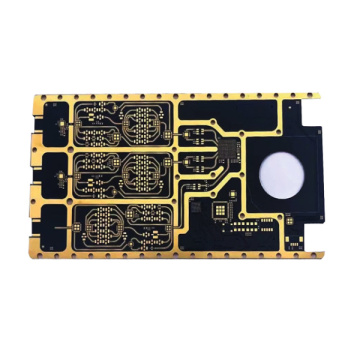


Quick Quality Multilayer Printed Circuit Board PCB (PCB8888)
-
$0.80≥1 Piece/Pieces
- Min. Order:
- 1 Piece/Pieces
- Min. Order:
- 1 Piece/Pieces
Your message must be between 20 to 2000 characters
Contact NowHow much is a custom PCB?
Before making the photosensitive metal base circuit board, we must first use Protel 99 SE to design the original PCB diagram, and then use the printer to print out the 1:1 film picture (or transparent sulfuric acid paper picture) of the PCB circuit board. It is best to choose a transparent film to print with a laser printer, so that the printed effect is very good, and it is fully qualified for general circuit board production requirements. If it is an inkjet printer, sulfuric acid paper is used, but the effect is poor. In this experiment, we used a laser printer to print out transparent film pictures.
The following picture shows the materials we used in the production process.
Materials
1. Cut the board, use a stationery knife to cut the circuit board into the size we need, and press it hard to break out the size we need.
Photosensitive plate with no protective film removed
2
3. Align the transparent film on the printed circuit layout with the photosensitive board, and pay attention to contact the print surface with toner on the film to the photosensitive circuit board to obtain the highest resolution. After the alignment is complete, cover a piece of glass on the top, the purpose is to make the transparent film and the circuit board close contact.
Put another piece of glass at a distance of about 10cm. This piece of glass is placed for the convenience of placing the lamp directly above the Low Cost Prototype PCB. Place an energy-saving light bulb on the glass and prepare for exposure.
It is best to use PHILIPS 14W energy-saving lamps for exposure, and the exposure time is 10 minutes. During the 10 minutes of exposure, we will prepare the developer solution. The developer is prepared according to the ratio of developer to water at 1:20. That is to say, 1g developer puts 20cc of water, of course, the concentration is higher and lower is not very relevant. It just affects the development time.
Put the lamp
Start exposure
3
Developer
Put the developer in the container
Add water to make a developer solution for later use
After ten minutes of exposure, put the Flame resistant PCB in the developer solution. As soon as I put it in, I saw a vague outline of the circuit displayed.
Circuit board put in developer
This step of development does not take much time, it will be completed in about a minute.
mulit-wiring printed boardafter development
The board that has been cleaned after development
4
Corrosion now begins.
The materials needed at this stage are concentrated hydrochloric acid (molecular mass 36.46) and hydrogen peroxide. Note that it is concentrated hydrochloric acid, the kind of white mist coming out when the lid is opened. Don't buy the hydrochloric acid used to wash toilets.
hydrochloric acid
Clean water, hydrochloric acid, and hydrogen peroxide are mixed into a corrosive solution in a ratio of about 6:3:1. The special feature of this corrosive solution is that its color is transparent, so that you can easily see the corrosion progress of the board. And the corrosion rate is much faster than ferric chloride. The pungent smell of hydrochloric acid is a little stronger.
Clean water, hydrochloric acid, and hydrogen peroxide are mixed into a corrosive solution in a ratio of about 6:3:1. The special feature of this corrosive solution.


Related Keywords