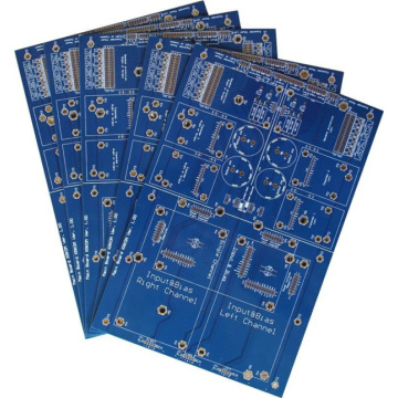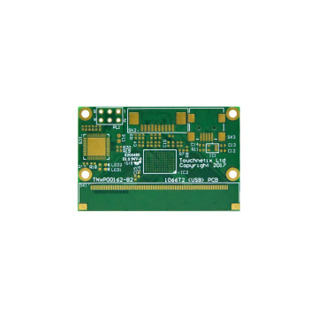
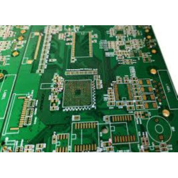
35um Copper Thickness Bare PCB with Drilling Holes
-
$1.02≥1 Piece/Pieces
- Min. Order:
- 1 Piece/Pieces
- Min. Order:
- 1 Piece/Pieces
Quantity:
Your message must be between 20 to 2000 characters
Contact NowBasic Info
Basic Info
Product Description
Product Description
What is PCBA manufacturing?
Electronic products must be mixed assembly before Box Build Assembly, and PCBA is used at this time, so PCB assembly is PCBA. PCBA is the abbreviation of Printed Circuit Board + Assembly in English. Simply put, the empty PCB board is loaded by SMT. Then go through the entire process of DIP plug-in, referred to as PCBA. In layman's terms, PCB is a circuit board with no upper components, and PCBA is a circuit board with soldered electronic components.

1. PCBA processing single-sided surface assembly process: solder paste printing-patch-reflow soldering;
2. PCBA processing double-sided surface assembly process: A side printing solder paste-patch-reflow soldering-flip board-B side printing solder paste-patch-reflow soldering;
3. PCBA processing single-sided mixed assembly (SMD and THC are on the same side): solder paste printing-patch-reflow soldering-manual plug-in (THC)-wave soldering;
4. Single-sided mixed assembly (SMD and THC are respectively on both sides of the PCB): B side printing red glue-patch-red glue curing-flap-A side plug-in-B side wave soldering;
5. Double-sided mixing device (THC has SMD on side A, and SMD on both sides of A and B): Printed solder paste on side A-patch-reflow soldering-flipping board-printed red glue on side B-patch-red glue curing-flipping Board—A side plug-in—B side wave soldering;
6. Double-sided mixed packaging (SMD and THC on both sides of A and B): Printed solder paste on side A-patch-reflow soldering-flip board-printed red glue on side B-patch-red glue curing-flip board-A Surface plug-in—B-side wave soldering—B-side plug-in is attached.


Related Keywords
Related Keywords
You May Also Like
You May Also Like