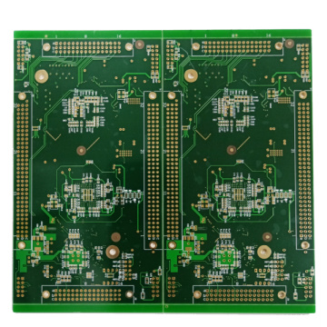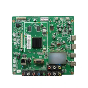
Direct Supply Portable PCBA Service
-
$0.50≥1 Piece/Pieces
- Min. Order:
- 1 Piece/Pieces
- Min. Order:
- 1 Piece/Pieces
Your message must be between 20 to 2000 characters
Contact NowIs PCB design in demand?
PCB has become the "mother of electronic products", and its applications have penetrated almost into various terminal fields of the electronics industry, including computers, communications, consumer electronics, industrial control, medical instruments, defense and military industry, aerospace and many other fields. The following is a detailed explanation of the PCB design process compiled by the Quick-turn PCB Prototypes Academy.
1. Preliminary preparation
Including the preparation of component libraries and schematic diagrams. Before proceeding with PCB design, we must first prepare the schematic SCH component library and PCB component packaging library.
The PCB Electronic components package library is best established by the engineer based on the standard size data of the selected device. In principle, establish the PC component package library first, and then establish the schematic SCH component library.
PCB component package library requirements are high, which directly affects the installation of PCB; schematic diagram SCH component library requirements are relatively loose, but pay attention to define the pin attributes and the corresponding relationship with the PCB component package library.
2. PCB structure design
According to the determined High frequency board size and various mechanical positioning, draw the PCB frame in the PCB design environment, and place the required connectors, buttons/switches, screw holes, assembly holes, etc. according to the positioning requirements.
Fully consider and determine the wiring area and non-wiring area (such as how much area around the screw hole belongs to the non-wiring area).
3. PCB layout design
The layout design is to place the electronic components in the PCB frame according to the design requirements. Generate the netlist (Design→Create Netlist) in the schematic tool, and then import the netlist (Design→Import Netlist) in the PCB software. After the netlist is successfully imported, it will exist in the background of the software. Through the Placement operation, all devices can be called out, and there is a flying line prompt connection between the pins. At this time, the layout design of the device can be carried out.
PCB layout design is the first important process in the entire PCB design process. The more complex the PCB board, the better the layout can directly affect the difficulty of later wiring.
Layout design depends on the circuit board designer's basic circuit knowledge and rich design experience, which is a higher level requirement for the circuit board designer. Elementary circuit board designers have little experience and are suitable for small module layout design or PCB layout design tasks with lower overall board difficulty.
4. PCB wiring design
PCB layout design is the process with the largest workload in the entire PCB design, which directly affects the performance of the custom pcb fabrication.


Related Keywords