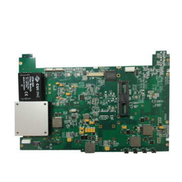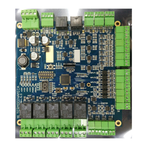
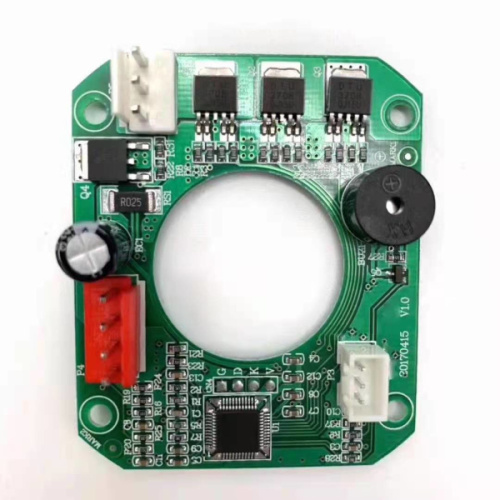
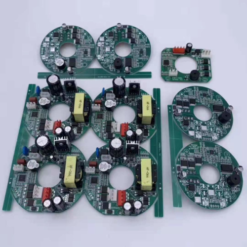
FPC for wearable Communication Devices PCB
-
$22.00≥1 Piece/Pieces
- Min. Order:
- 1 Piece/Pieces
- Min. Order:
- 1 Piece/Pieces
Your message must be between 20 to 2000 characters
Contact Now
Is PCB design difficult?
It is not difficult to learn PCB design. The software is just a tool. If you have a computer foundation, you can learn how to use PCB software in two weeks. The key is to understand electronic circuits.
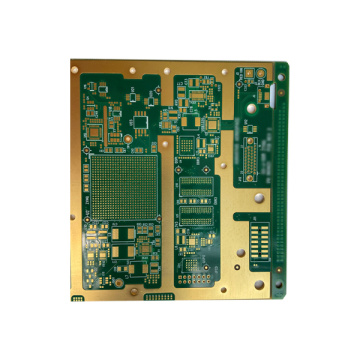
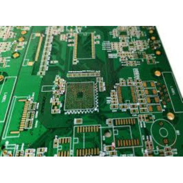
When it comes to PCB, many friends will think that it can be seen everywhere around us, from all household appliances, various accessories in computers, to various digital products, as long as it is electronic products, almost all use PCB, so what is PCB? ? PCB is Printed Circuit Block, that is, printed circuit board, for Surface-Mount (SMT) &BGA Assembly, the base version with circuit. By using a printing method, the copper-plated base plate is printed on the anti-corrosion circuit, and the circuit is etched and washed out.
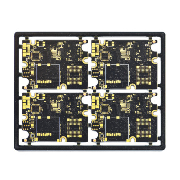
PCB can be divided into single-layer board, double-layer board and 0-18Layer FR4 board. Various electronic components are integrated on the PCB. On the most basic single-layer PCB, the parts are concentrated on one side, and the wires are concentrated on the other side. In this way, we need to make holes in the board so that the pins can pass through the board to the other side, so the pins of the parts are soldered to the other side.
Because of this, the front and back sides of such a PCB are called the part side and the solder side respectively. The double-layer board can be regarded as a combination of two single-layer boards relative to each other, and there are Electronic Components and wiring on both sides of the board. Sometimes it is necessary to connect a single wire on one side to the other side of the board, which requires a via hole. A via is a small hole filled or coated with metal on the PCB, which can be connected with the wires on both sides. Many computer motherboards now use 4-layer or even 6-layer PCBs, while graphics cards generally use 6-layer PCBs. Many high-end graphics cards like the nVIDIAGeForce4Ti series use 8-layer PCBs. This is the so-called multi-layer PCB. On the 0-18Layer FR4 board, the problem of connecting the lines between the various layers will also be encountered, which can also be achieved through vias.
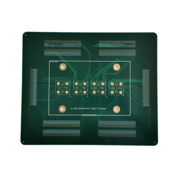
Because it is a multilayer PCB, sometimes vias do not need to penetrate the entire PCB. Such vias are called buried vias and blind vias, because they only penetrate a few layers. A buried PCB connects several layers of internal PCB with the surface PCB without having to penetrate the entire board. The blind via hole PCB only connects to the internal PCB, so it is invisible from the surface. In a multilayer PCB, the entire layer is directly connected to the ground wire and the power supply.
So we classify each layer as signal layer, power layer or ground layer. If the parts on the PCB require different power supplies, this type of PCB usually has more than two layers of power and 4 Layer Power line Circuits. The more PCB layers used, the higher the cost. Of course, the use of more layers of PCB is very helpful to provide signal stability.


Related Keywords