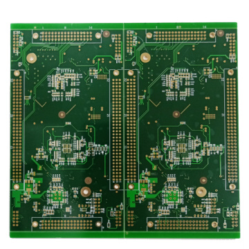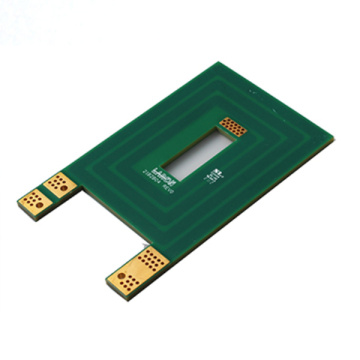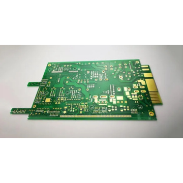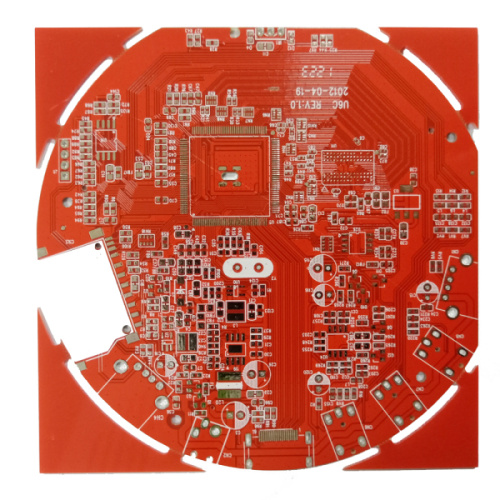


12-layer HDI PCB 1.6mm FR4-TG170 Immersion Finish
-
$8.30≥1 Piece/Pieces
- Min. Order:
- 1 Piece/Pieces
- Min. Order:
- 1 Piece/Pieces
Quantity:
Your message must be between 20 to 2000 characters
Contact NowBasic Info
Basic Info
Product Description
Product Description
Where are HDI PCBs used?
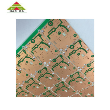
High-density interconnect HDI PCB represents one of the fastest growing segments of the printed circuit board market. Due to the higher circuit density of HDI PCB, thinner lines and spaces, smaller through holes and capture pads, and higher connection pad density can be incorporated in the design. HDI PCBs have blind via hole PCBs and buried PCBs, and usually contain micro-holes with a diameter of 0.006 or less. So, what are the main applications of HDI PCB circuit boards?

The development of HDI PCB technology has brought unprecedented design freedom and flexibility to engineers, allowing more PCB assemblies to be placed on both sides of the original PCB as needed, while allowing smaller components to be placed together. This means that HDIPCB will eventually lead to faster signal transmission and enhanced signal quality.
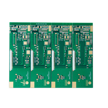
HDI PCB is widely used to reduce the weight and overall size of products, and to enhance the electrical performance of equipment; it often appears in mobile phones, touch screen devices, notebook computers, digital cameras, and 4G network communications. HDI PCB is also prominent in medical equipment and various electronic aircraft parts.

HDI PCB is suitable for various industries. As mentioned above, you will find them in all types of digital devices such as smartphones and tablets, and miniaturization is the key to the effective application of products. You can also find it in cars, airplanes and other vehicles that rely on electronics.


Related Keywords
Related Keywords
You May Also Like
You May Also Like