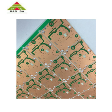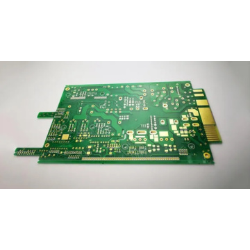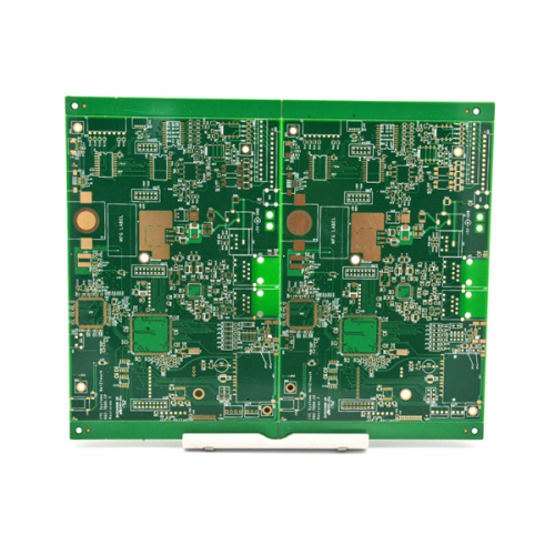
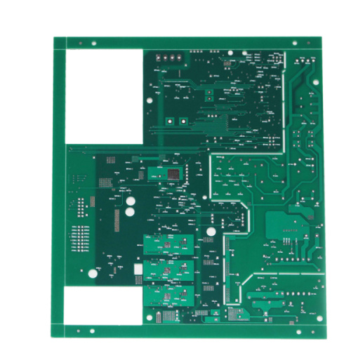
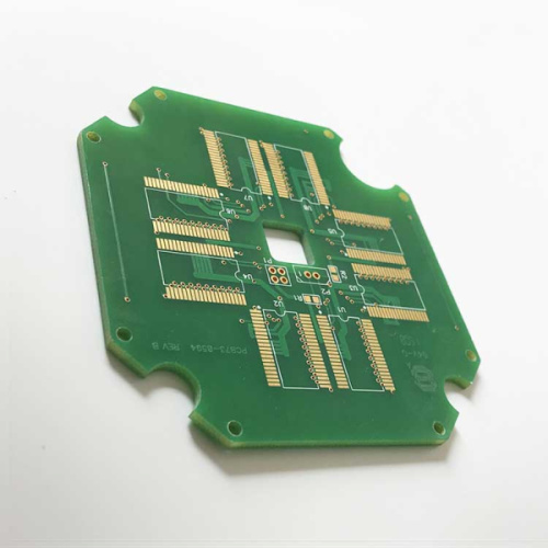
Green solder mask high frequency custom pcb
-
$8.30≥1 Piece/Pieces
- Min. Order:
- 1 Piece/Pieces
- Min. Order:
- 1 Piece/Pieces
Your message must be between 20 to 2000 characters
Contact Now
What is a solder mask?
The solder mask can actually be called a window layer or a green oil layer. It also has an English name-solder mask. It refers to the place where the green oil is to be spread on the pcb, and this solder mask uses a negative output, so after the shape of the solder mask is mapped to the board, it is not the green oil solder mask, but the copper exposed Skin. Expose the copper skin, we will habitually call the window.

The basic structure of a printed circuit board is pads, vias, solder mask, and text printing. The solder mask is the yellow or red or black or green or other colors that you see. Some boards are yellow solder mask. In PCBA Manufacturing, the role of the solder mask is to prevent the parts that should not be soldered from being connected by solder. Reflow soldering is achieved by the solder mask. The hot tin water on the entire surface of the board, the exposed circuit board without the solder mask is wetted and soldered, and the part with the solder mask is not wetted.

The solder mask can prevent the conductive solder bridging between various Electronic Components. In essence, it blocks the short circuit. The different PCB solder masks are as follows.
Top and bottom masks: Electronic engineers know all kinds of openings. He knows what has been added through ink, epoxy or thin film technology. Then, he was able to solder the component pins on the board with the assistance of the confirmed orientation. You can also notice the conductive trace pattern on the top of the circuit board. Call these top tails. The lower one is the bottom mask.
Epoxy liquid: If you want a cheap choice, please choose epoxy liquid. There are many applications for thermosetting polymers. Silk screen is a printing technology. It uses a woven mesh to support the ink blocking pattern. The grid can create an open area for ink transport.
Liquid ink can be photographed and imaged: We supply solder mask as ink formulation. Ability to spray ink into PCB. Then, be able to expose the pattern and develop it. It is important to note that the process and liquid ink formulations are used. This requires a clean environment free of pollutants and particles. People can remove it after exposing it to ultraviolet light. This is done through a high-pressure water spray called developer.


Related Keywords