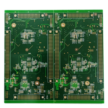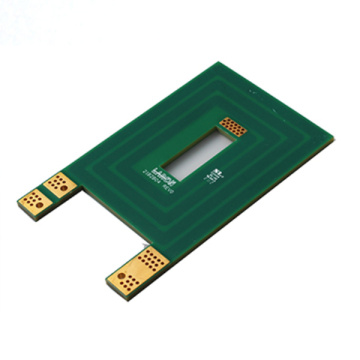


2 Layers Rogers High Frequency Ceramic Pcb
-
$8.30≥1 Piece/Pieces
- Min. Order:
- 1 Piece/Pieces
- Min. Order:
- 1 Piece/Pieces
Your message must be between 20 to 2000 characters
Contact Now
What are the advantages of HDI in PCB?
HDI stands for high-density interconnection, and this technology is rapidly becoming popular in the field of printed circuit boards. Generally speaking, HDI PCB can bring a series of benefits to technology. After all, they help simplify circuit boards so that they can be made more and take up less space. This means that boards tend to be smaller, which means that electronic devices that use these types of boards tend to be smaller. They can perform well, but they have smaller, more simplified packages. Consider how many different types of devices have become smaller and smaller in the past decade. One of the reasons is to use HDI PCB.
These boards can provide a large number of interconnections in a small space. The placement of the components on the board is closer, which helps to reduce the size, but the function is the same as the larger board. If a board has 120 to 160 pins per square inch, then it is an HDI PCB. When using universal wiring, the components are placed together. With the help of microvia technology and buried and blind vias, these types of boards are made possible. They are very efficient and are becoming more and more popular in a variety of different industries, as shown below.

Many people want to find a way to reduce product manufacturing area, and one of the best ways is to use HDI PCB. They are a good solution when you need to reduce the size and weight and still need functionality and reliability of the product. One of the other advantages of these circuit boards is that they use solder-in-pad technology and blind via technology. This allows components to be put together, thereby shortening the length of the signal path, which helps provide faster and more reliable signals because these paths are shorter.
Even though these boards can provide many advantages, you will still find that they are still very affordable. For those looking for reliable and durable options for their electronic equipment, this is a cost-effective solution. Nevertheless, to determine if they are suitable for you, it is important to learn more about them and how to use them. You also need to understand the difference between conventional printed circuit boards and HDI printed circuit boards.

Because of the benefits they provide, you will find that HDI PCBs are used in various electronic devices in many different industries. The medical industry is one of the most famous industries. Medical devices manufactured today generally need to be smaller. Whether it is a piece of equipment in a laboratory or an implant, a smaller size is often a better choice, and HDI PCB can provide a great help in this regard. Pacemakers are a good example of the types of products that use these types of PCBs. Many types of surveillance and detection equipment (such as endoscopes or colonoscopes) use this technology. Again, in these cases, smaller is the better choice.
In addition to the healthcare sector, the automotive industry also uses HDI PCB. In order to maximize the use of available space in cars, they are making certain electronic components smaller. Of course, tablets and smartphones use this technology. This is why many of these devices have become thinner and lighter as they develop.
You will also find HDI PCBs for aerospace and military applications. Their reliability and small size allow them to be used in many different applications. In the future, more and more devices from different fields may use this technology.

To better understand some of the main differences between these two options, consider the following list.
HDI PCB has denser components per square inch
Compared to typical PCBs, these boards are ultimately smaller and lighter
They use lasers to drill directly, while standard PCBs are usually mechanically drilled
Both the number of layers and the aspect ratio tend to decrease
These are some of the differences between HDI PCB and conventional PCB. However, this does not mean that the HDI option is always the right choice for you. Take the time to consider the project you are working on, and then determine which option best suits your needs.
Design HDI PCB correctly
Although using one of these types of PCBs seems to be the perfect solution for your needs, if you want to realize all the benefits they can convey, it is important to understand how to design them correctly. For these types of designs, if possible, you will want to ensure that the number of layers used in the sequence does not exceed three. Ideally, the number of sequential laminations should be small.


Related Keywords