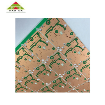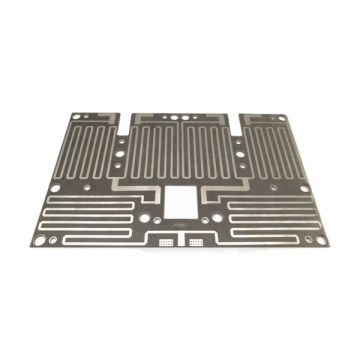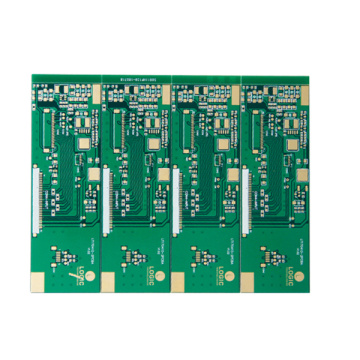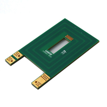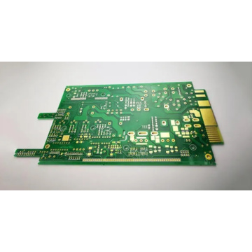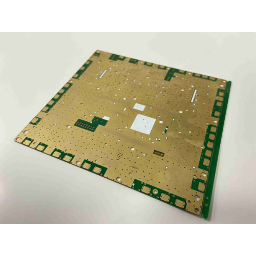
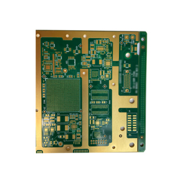
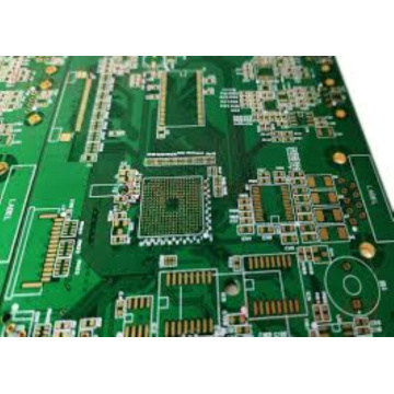
High Frequency ceramic Board, PCB
-
$10.30≥1 Piece/Pieces
- Min. Order:
- 1 Piece/Pieces
- Min. Order:
- 1 Piece/Pieces
Your message must be between 20 to 2000 characters
Contact Now
What is heavy copper PCB?
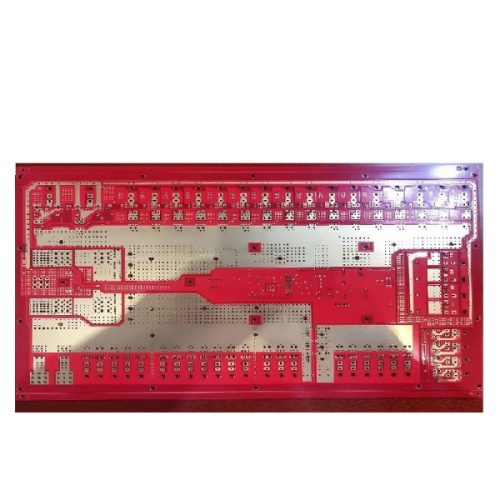
Heavy copper PCBs are widely used in electronics and circuits that require high power transmission. Heavy copper PCBs are manufactured with 4 ounces or more of copper on each layer. 4 ounce copper PCBs are most commonly used in commercial products. The concentration of copper can be as high as 200 ounces per square foot. In addition, the thermal strength provided by these PCBs is impeccable. In many applications, especially in electronic products, the thermal range is critical, because high temperatures cause severe damage to sensitive Electronic Components and severely affect circuit performance. Heavy copper PCBs are widely used in various products because they provide multiple functions to improve circuit performance. These PCBs are widely used in high-power equipment such as transformers, radiators, inverters, military equipment, solar panels, automotive products, welding equipment, and power distribution systems. Heat dissipation is essential for the development of rugged circuits. Improper thermal signal processing will not only affect the performance of electronic equipment, but also shorten the service life of the circuit.
Heavy copper PCB can be used to develop high-power circuit wiring. This wiring mechanism provides more reliable thermal stress treatment, and provides fine processing, while integrating multiple channels on a single-layer compact board.

Just like the standard PCB manufacturing method, heavy copper PCB manufacturing requires more delicate processing.
Traditional heavy copper PCBs are manufactured using outdated technology, resulting in uneven tracking and undercutting on the PCB, resulting in low efficiency. However, today, modern manufacturing technology supports fine cuts and minimal undercuts.
Thermal stress treatment quality of heavy copper PCB
When designing a circuit, factors such as thermal stress are very important, and engineers should eliminate thermal stress as much as possible.
Over time, PCB manufacturing processes have continued to evolve, and various PCB technologies have been invented, such as Aluminum LED boards, which can handle thermal stress.
It is in the interests of heavy copper PCB designers to minimize the power budget while maintaining the circuit. Performance and environmentally friendly design with heat dissipation performance.
Since the overheating of electronic components can lead to failures and even life-threatening, hazard management cannot be ignored.
The traditional process to achieve heat dissipation quality is to use external heat sinks, which are connected and used together with heat generating components. Since the heat-generating parts are close to high temperature if they do not dissipate heat, in order to dissipate this heat, the radiator consumes heat from the parts and transfers it to the surrounding environment. Usually, these heat sinks are made of copper or aluminum. The use of these radiators not only exceeds the development cost, but also requires more space and time. Although the result is not even close to the heat dissipation capacity of a heavy copper PCB.
In heavy copper PCBs, the heat sink is printed on the circuit board during the manufacturing process instead of using any external heat sink. Since the external radiator requires more space, there are fewer restrictions on the placement of the radiator.
Since the heat sink is plated on the circuit board and connected with the heat source using conductive through holes instead of any interfaces and mechanical joints, the heat is transferred quickly, thereby improving the heat dissipation time.
Compared with other technologies, the heat dissipation vias in heavy copper PCBs can achieve more heat dissipation because the heat dissipation vias are developed with copper. In addition, the current density is improved and the skin effect is minimized.

The advantages of heavy copper PCB make it the top priority for the development of high-power circuits. The heavy copper concentration can handle high power and high heat, which is why high-power circuits have been developed using this technology. Such circuits cannot be developed with low-copper concentration PCBs because they cannot withstand the huge thermal stresses caused by high currents and flowing currents. Heavy copper PCBs are generally considered high current PCBs because of their significant heat dissipation capabilities.
The relationship between PCB copper thickness and current is an important factor in the use of heavy copper PCBs. As the copper concentration increases, the total cross-sectional area of copper also increases, which reduces the resistance in the circuit. As we know, losses are devastating to any design, and copper concentration enables these PCBs to reduce power budgets.
Current conductivity is an important factor, especially when processing low-power signals, and the current conductivity of heavy copper PCBs is improved due to its extremely low resistance.
The connector is necessary for jumper connection. However, connectors are often difficult to maintain on traditional PCBs. Due to the low strength of occasional PCBs, the connector parts are usually affected by mechanical stress, but heavy copper PCBs provide higher strength and ensure higher reliability.

Heavy copper PCBs are manufactured on advanced automated machines, which allows us to develop highly reliable PCBs. So far, we have developed a two-layer PCB, up to 20 ounces, and a multilayer PCB with a copper weight of 4-6 ounces.


Related Keywords