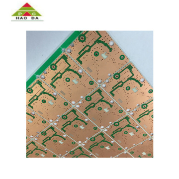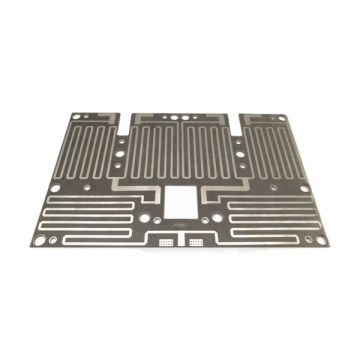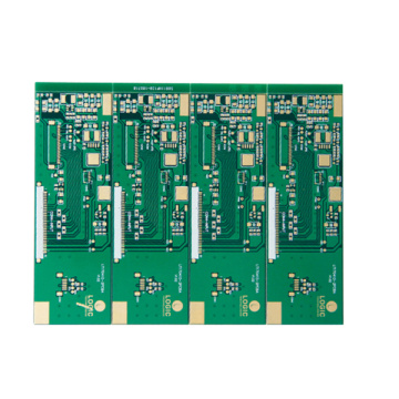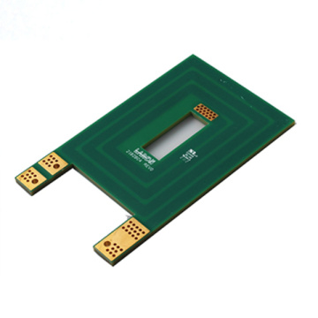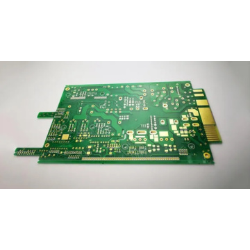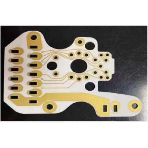
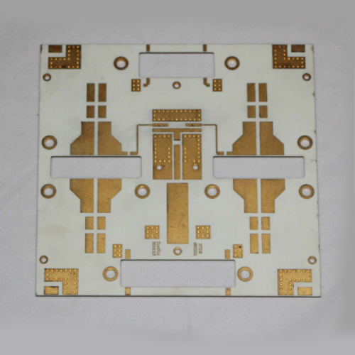
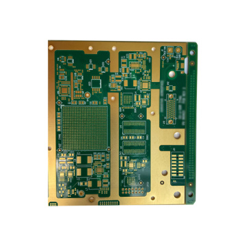
High Frequency ceramic PCBs
-
$10.30≥1 Piece/Pieces
- Min. Order:
- 1 Piece/Pieces
- Min. Order:
- 1 Piece/Pieces
Your message must be between 20 to 2000 characters
Contact Now
Why use ceramics for circuit boards?
Ceramic circuit boards are actually made of ceramics base copper-clad laminates, which can be made into various shapes. Among them, ceramics base copper-clad laminates have the most outstanding characteristics of high temperature resistance and high electrical insulation. They have the advantages of low dielectric constant, low dielectric loss, high thermal conductivity, good chemical stability, and similar component thermal expansion coefficients. Ceramic printed circuit boards are produced using laser rapid activation metallization technology LAM technology. Used in the LED field, high-power semiconductor modules, semiconductor coolers, electronic heaters, power control circuits, power hybrid circuits, smart power components, high-frequency switching power supplies, solid state relays, automotive electronics, communications, aerospace and military electronic components.

Main advantages:
1. Higher thermal conductivity
2. More matching thermal expansion coefficient
3. A harder, lower resistance metal film alumina ceramic circuit board
4. The solderability of the base material is good, and the use temperature is high.
5. Good insulation
6. Low frequency loss
7. Can be used for high-density PCB assembly
8. It does not contain organic ingredients, is resistant to cosmic rays, has high reliability in aerospace and aerospace, and has a long service life
9. The copper layer does not contain an oxide layer and can be used for a long time in a reducing atmosphere.

Why use ceramics for circuit boards?
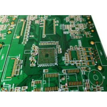
The ceramic circuit board is through the laser drilling process, the bonding force between the ceramic and the metal is high, does not fall off, foams, etc., and the effect of growth together, high surface flatness, roughness ratio of 0.1 micron to 0.3 micron, laser strike hole diameter From 0.15 mm to 0.5 mm, or even 0.06 mm. With the development of high-power electronic products in the direction of miniaturization and high-speed, traditional FR-4, Aluminum base board and other substrate materials are no longer suitable for the development of high-power and high-power. With the advancement of science and technology, the intelligent application of PCB industry. Traditional LTCC and DBC technologies are gradually replaced by DPC and LAM technologies. The laser technology represented by LAM technology is more in line with the development of HDI PCB and fineness. Laser drilling is the front-end and mainstream drilling technology in the PCB industry. The technology is efficient, fast, accurate, and has high application value. The bonding strength between the metal layer and the ceramic is high, the electrical properties are good, and the welding can be repeated. The thickness of the metal layer can be adjusted in the range of 1μm-1mm, which can achieve L/S resolution. 20μm, can be directly connected to provide customized solutions for customers.


Related Keywords