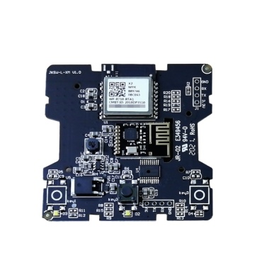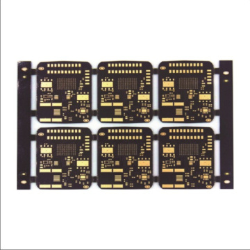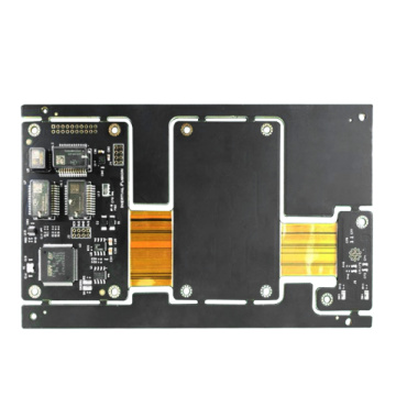


High Density Blind Buried Vias HDI pcb
-
$9.90≥1 Piece/Pieces
- Min. Order:
- 1 Piece/Pieces
- Min. Order:
- 1 Piece/Pieces
Your message must be between 20 to 2000 characters
Contact NowWhat is a high density PCB?
Introduction to high-density PCB soft board
1. Definition of high-density PCB soft board:
Generally, the high-density Rigid-Flex Board is defined by the process capability of fine lines and micro-holes. The line pitch (Pitch) is less than 150μm, and the micro-hole diameter is less than 150μm (the definition of IPC). The ultra-high-density PCB soft board is further reduced. The application of high-density PCB soft board can distinguish several fields:
A. originality electronics IC carrier board: such as CSP, BGA, etc.
B. Information products: such as Hard Disk, Ink Jet Printer
C. Consumer products: such as cameras (Camera), mobile phones (Mobile Phone)
D. Office automation products: such as Facsimile Machine
E. Medical products: such as hearing aid (Hearingaid), electric shock device (Defibrillator)
F. LCD module
In order to maintain high growth rates and profits, flexible substrates will inevitably develop towards high-scale applications. At this time, improvements and breakthroughs in materials must be made at the same time. Among them, non-adhesive base materials and photosensitive protective film will act as traditional flexible substrates. Enter the important role of high-density PCB soft boards. China has a good foundation in IC and LCD assembly, and there is also a certain level of custom pcb fabrication capability and scale. If it can be matched with the domestic IC and LCD panel manufacturing capabilities that have been deeply cultivated, it will be in the creation of new assembly products and technologies. There should be great opportunities and niches.


Related Keywords