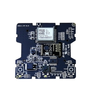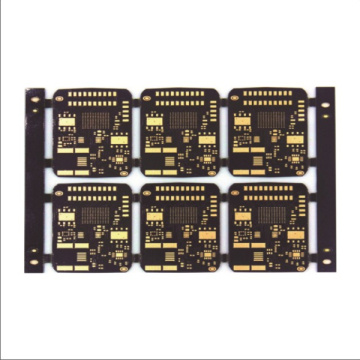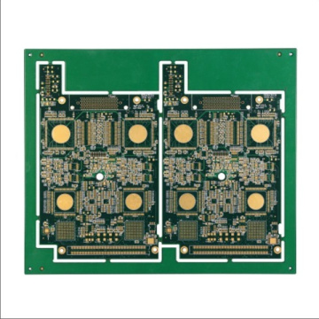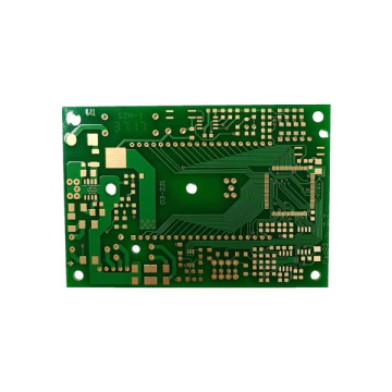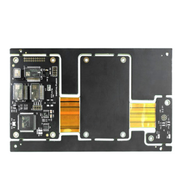


High Density Interconnect PCB Electronics
-
$120.00≥1 Piece/Pieces
- Min. Order:
- 1 Piece/Pieces
- Min. Order:
- 1 Piece/Pieces
Quantity:
Your message must be between 20 to 2000 characters
Contact NowBasic Info
Basic Info
Product Description
Product Description
What is VIA in PCB?
In custom pcb fabrication, vias are called vias, which are divided into through holes, blind holes and buried holes. They are mainly used to connect wires in different layers of HDI High Quality PCB Products in the same network. They are generally not used for soldering Electronic Components. in:
1) Blind holes are used for the connection of the surface circuit and the inner circuit (blind via hole PCB only exists, that is, only one head of the hole can be seen, and the other head does not penetrate the board).
2) Buried vias are the connections between inner and inner circuits (only available in buried PCBs, buried vias cannot be seen outside)
3) Through holes are holes that penetrate the surface and bottom layers and are used for internal interconnection or as installation positioning holes for Electronic Components.
The only used for the connection of the circuit is the via hole, which is small in size. Holes used to install and solder Electronic Components are generally larger than via holes.
Vias consist of drilled holes and pads.
The simple understanding is: the pad is a larger hole for soldering Electronic Components. The via is very small, just a hole that connects lines of different layers.
In simple terms:
1) Vias are holes that connect and conduct between layers in double or multiple layers; they are characterized by electrical conduction and are not used for welding;
2) Drilling is a mechanical hole on the PCB board, which is used for assembly. It does not necessarily have electrical properties and cannot be soldered;
3) The pad is used to fix the perforated or gold-plated surface of Electronic Components (surface pad SMD PAD), which is characterized by electrical conductivity and can be soldered.


Related Keywords
Related Keywords
You May Also Like
You May Also Like