


Hdi Pcb Pcba One stop Service
-
$120.00≥1 Piece/Pieces
- Min. Order:
- 1 Piece/Pieces
- Min. Order:
- 1 Piece/Pieces
Your message must be between 20 to 2000 characters
Contact Now
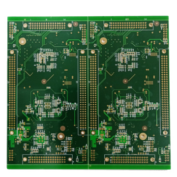
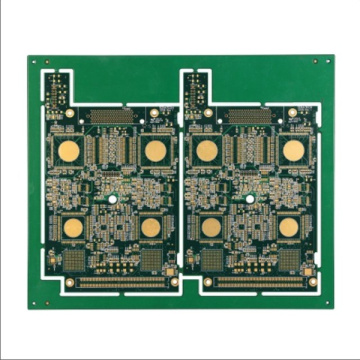
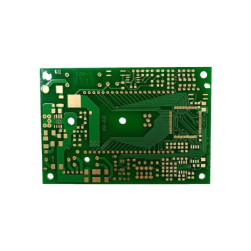
What is HDI technology?
HDI PCB refers to High Density Interconnect, or mulit-wiring printed board, which is a relatively new technology developed in the PCB industry at the end of the 20th century.
The traditional PCB board drilling is affected by the drill, when the drilling hole diameter reaches 0.15mm, the cost is already very high, and it is difficult to improve again. The drilling of HDI PCB no longer relies on traditional mechanical drilling, but uses laser drilling technology. (So it is sometimes called a laser board.) The hole diameter of HDI PCB is generally 3-5mil (0.076-0.127mm), the line width is generally 3-4mil (0.076-0.10mm), and the size of the pad can be greatly improved. As a result, more circuit distribution can be obtained per unit area, and high-density interconnection comes from this.
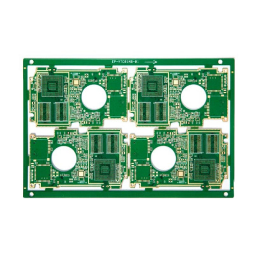
The emergence of HDI PCB technology has adapted and promoted the development of the PCB industry. This makes it possible to arrange denser BGA, QFP, etc. in the HDI PCB. At present, HDI technology has been widely used, among which the first-order HDI has been widely used in PCB production with 0.5PITCH BGA.
The development of HDI technology promotes the development of origin electronics IC technology, and the development of origin electronics IC technology in turn promotes the improvement and progress of HDI technology.
At present, 0.5PITCH BGA chips have been gradually adopted by design engineers. The solder fillets of BGA have also gradually changed from the form of hollowing out the center or the form of center grounding to the center with signal input and output requirements.


Related Keywords