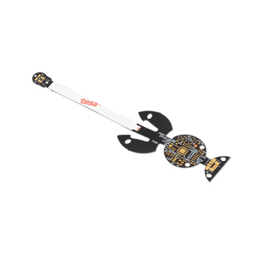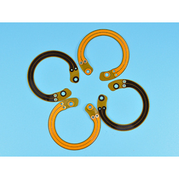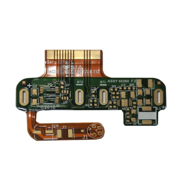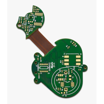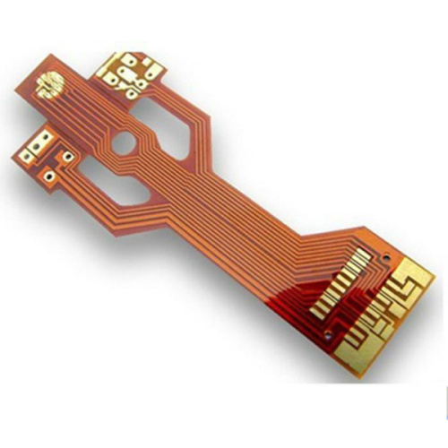
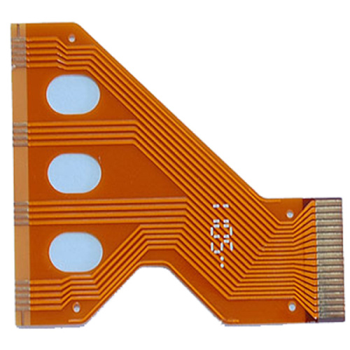
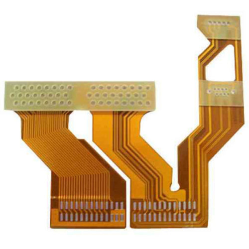
Rigid-Flexible PCB and Flexible Pcbs
-
$6.10≥5 Piece/Pieces
- Min. Order:
- 5 Piece/Pieces
- Min. Order:
- 5 Piece/Pieces
Your message must be between 20 to 2000 characters
Contact NowWhat is a rigid PCB?
In PCB assembly, printed circuit boards (Printed Circuit Boards) are a key part. It is equipped with other Electronic Components and connected to the circuit to provide a stable circuit working environment. For example, the circuit configuration can be divided into three categories:
[Single panel] Arrange the metal lines that provide the connection of the parts on an insulating substrate material, which is also a support carrier for installing the parts.
[Double-sided board] When the single-sided circuit is not enough to provide the connection requirements of electronic parts, the circuit can be arranged on both sides of the substrate, and through-hole circuits can be deployed on the board to connect the circuits on both sides of the board. The raw materials of rigid circuit boards are cardboard, fireproof board and corrugated fiber board. English name (FR-4 PCB)
[Multilayer board] In the case of Through-Hole Assembly's more complex application requirements, the circuit can be arranged into multiple layers of nodules and pressed together (such as high frequency mixing pressure plate) together, and through-hole circuits are arranged between the layers to connect All layers of circuits.

Multilayer circuit board
In custom pcb fabrication, the copper foil substrate is first cut into a size suitable for processing and production. Before laminating the substrate, it is usually necessary to properly roughen the copper foil on the surface of the board by brushing, microetching, etc., and then attach the dry film photoresist closely to it at an appropriate temperature and strength. Send the dry film photoresist substrate to the UV exposure machine for exposure. The photoresist will undergo polymerization in the light-transmitting area of the negative film after being irradiated by ultraviolet light (the dry film in this area will be affected by the later development and copper etching steps. Keep it as an etching resist), and transfer the circuit image on the negative to the dry film photoresist on the board. After tearing off the protective film on the membrane surface, the unlit area on the membrane surface is moistened with a sodium carbonate aqueous solution, and then the exposed copper foil is corroded and removed with a mixed solution of hydrochloric acid and hydrogen peroxide to form a circuit. Finally, the dry film photoresist that has worked well is washed away with sodium hydroxide aqueous solution. For inner circuit boards with more than six layers (inclusive), an automatic positioning punching machine is used to punch out the riveting reference holes for the alignment of the interlayer circuits.

The finished inner circuit board must be laminated with the outer circuit copper foil with glass fiber resin film. Before pressing, the inner layer board needs to be blackened (oxidized) to make the copper surface to increase the insulation; and the copper surface of the inner layer circuit is roughened to produce good bonding performance with the film. When the 0-18Layer FR4 board is pressed, the inner circuit boards of the six layers (including) or more are riveted in pairs with a riveting machine. Then use the tray to neatly press it between the mirror steel plates, and send it to the vacuum laminator to harden the film with proper temperature and pressure. The laminated circuit board is locked out with an X-ray automatic positioning and locking machine, and the hole is used as a reference hole for the alignment of the inner and outer layers. And make appropriate fine cutting of the edge of the board to facilitate subsequent processing.


Related Keywords