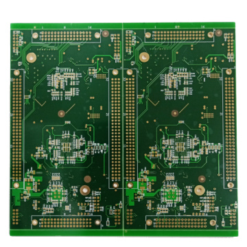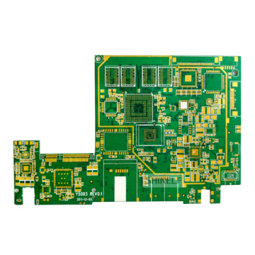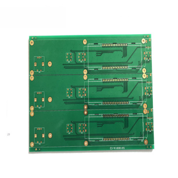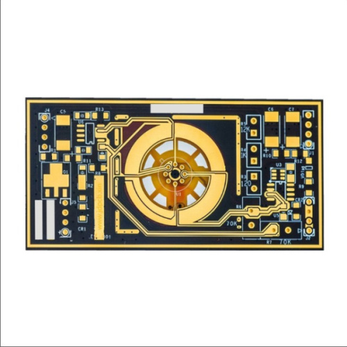
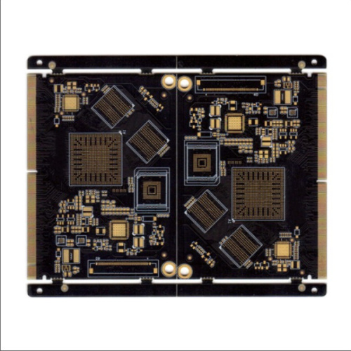
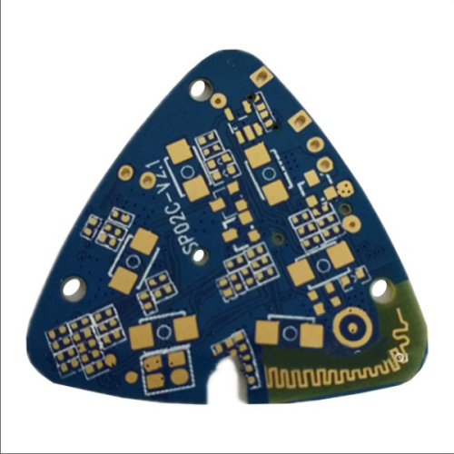
flame resistant fibre PCB
-
$0.10≥1 Piece/Pieces
- Min. Order:
- 1 Piece/Pieces
- Min. Order:
- 1 Piece/Pieces
Quantity:
Your message must be between 20 to 2000 characters
Contact NowBasic Info
Basic Info
Product Description
Product Description
What is multilayer PCB manufacturing?
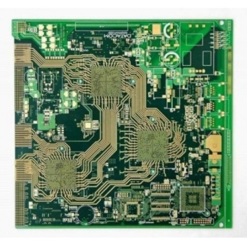
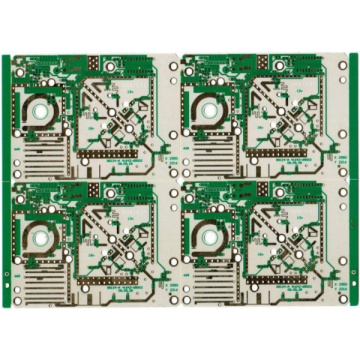
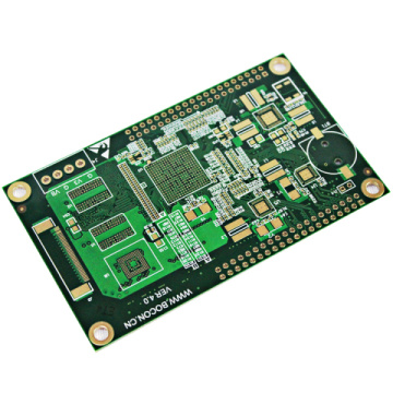
The printed circuit board (PCB) is one of the most important parts of an electronic circuit and contributes to its performance. Of course, as with the operation of the PCB, it is also important to understand the manufacturing process. Since 60% of PCBs used in industrial electronic circuits are multilayered, the manufacturing process of multilayer PCBs has become a topic of concern. The demand for smaller, more powerful and faster devices has driven the demand for multilayer PCBs. Copper is used as the conductor of these PCBs, which contributes to their current-carrying capacity.


Related Keywords
Related Keywords
You May Also Like
You May Also Like