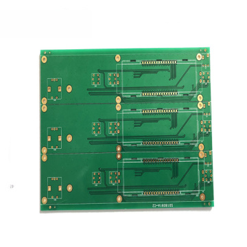


Flame retardant fiberglass PCB
-
$0.13≥1 Piece/Pieces
- Min. Order:
- 1 Piece/Pieces
- Min. Order:
- 1 Piece/Pieces
Your message must be between 20 to 2000 characters
Contact NowWhat is the density of FR4?
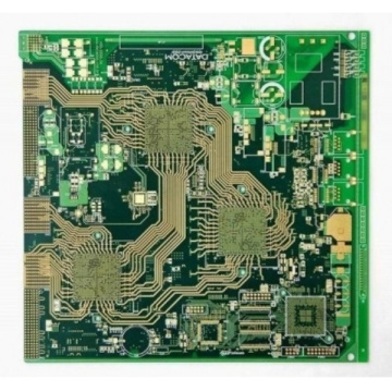
The density of Flame resistant PCB 4-layer fr4 custom pcb fabrication is generally between 1.05-1.2, the size is 240x420mm, and the weight of 1.6mm thickness is about =24*24*0.16*1.1=100 grams.
PCB is a provider of electrical connections for electronic components. Its development has a history of more than 100 years; its design is mainly layout design; the main advantage of using PCB is to greatly reduce wiring and assembly errors, and increase the level of automation and production labor rate. According to the number of layers of custom pcb fabrication, it can be divided into single-sided board, double-sided board, four-layer board, six-layer board and 0-18Layer FR4 board.
The 4-layer FR4 PCB is a printed board formed by laminating and bonding alternate conductive pattern layers and insulating material layers. The number of conductive pattern layers is more than two, and the electrical interconnection between the layers is realized through metallized holes. The connection line of the multilayer printed board is short and straight, which is convenient for shielding, but the process of the printed board is complicated, and the reliability is slightly worse due to the use of metalized holes. It is often used in computer boards.
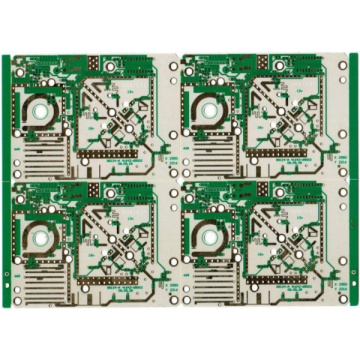
For the production of circuit boards, the more layers there are, the more production procedures there will be. Of course, the failure rate will increase, and the cost will increase relatively. Therefore, multi-layer boards are only used in advanced circuits.
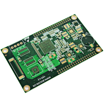
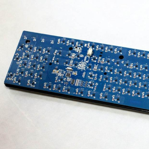
Usually on the circuit board, the components are placed on the top layer, so the top layer is generally called the component surface, and the bottom layer is generally used for soldering, so it is also called the soldering surface. For SMD components, components can be placed on both the top and bottom layers. Components are also divided into two categories, pin-type components and surface-mount components (SMD).


Related Keywords