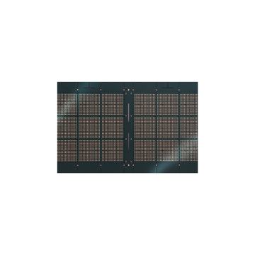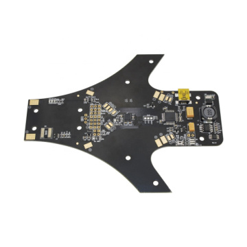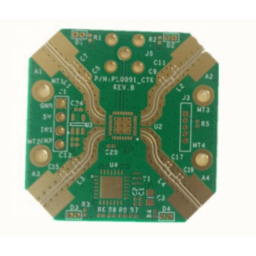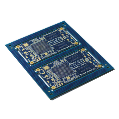


Fr4 6 Layer PCB/PCBA Prototype Manufacturing
-
$0.95≥1 Piece/Pieces
- Min. Order:
- 1 Piece/Pieces
- Min. Order:
- 1 Piece/Pieces
Your message must be between 20 to 2000 characters
Contact NowWhat are multi layer PCBs used for?
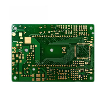
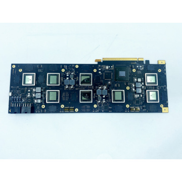
The biggest difference between PCB multi-layer boards and single-sided and double-sided boards is the addition of internal power and ground planes. The power supply and ground network are mainly routed on the power supply layer. There are conductive metals on both sides of each substrate layer on the PCB multilayer board, and a special adhesive is used to connect the boards together, such as a high frequency mixing pressure plate. And there are insulating materials between each board. However, PCB multilayer wiring is mainly based on the top and bottom layers, supplemented by intermediate wiring layers.
Therefore, the design of the multilayer PCB board is basically the same as the design method of the double-sided board. The key is how to optimize the wiring of the internal electrical layer to make the wiring of the circuit board more reasonable. The inevitable product of PCB assembly multifunctional development, large capacity and small volume.

(Buried PCB) and heavy copper pcb
(High plate thickness aperture ratio), which can meet market demand. PCB multilayer printed boards are widely used in the manufacture of electronic products due to their flexible design, stable and reliable electrical performance and excellent economic performance.


PCB multilayer printed boards are widely used in the manufacture of electronic products due to their flexible design, stable and reliable electrical performance and excellent economic performance. Blind hole technology, high plate thickness to aperture ratio and other blind technology can meet market demand. PCB multilayer printed boards are widely used in the manufacture of electronic products due to their flexible design, stable and reliable electrical performance and excellent economic performance.


Related Keywords