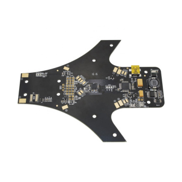


device communication control pcb
-
$0.25≥1 Piece/Pieces
- Min. Order:
- 1 Piece/Pieces
- Min. Order:
- 1 Piece/Pieces
Quantity:
Your message must be between 20 to 2000 characters
Contact NowBasic Info
Basic Info
Product Description
Product Description
Can tracks on PCB cross each other?
In the double-sided PCB board, the front and back wiring can be used to solve the problem when the wiring is crossed. In single-sided PCB design, jumper wires are often used when some lines cannot be connected. For beginners, jumper wires are often random, with long and short ones, which will cause inconvenience in production. When placing jumper wires, the fewer types, the better, usually only 6mm, 8mm, and 10mm are available. Those outside this range will cause inconvenience in production. In addition, there are the following methods to make the wires cross and realize the role of jumper wires.
1. Add cross-line or zero-ohm resistance. Connecting wires on the reverse side of the PCB is called a jumper. If the length of the jumper in the same circuit board is not uniform, it will affect the appearance. The length of the jumper should be consistent with small components (such as resistors). If the zero-ohm resistor is installed, it will be more tidy, so that people will not feel the existence of cross-line.
2, PCBA component substitution method. For example, a jumper is connected in series with an 18KΩ resistor, now the resistance is changed to 15KΩ, a 3KΩ resistor is installed at the jumper, the total value is still 18kΩ, and the PCB jumper is cancelled.
3. Printing cross-line. The single-sided PCB can be crossed by printing the crossover, but the manufacturing cost of the printed board will increase slightly.
4. Labyrinth wiring. In low-speed digital circuits, in order to be able to route on the same printed board surface, the labyrinth wiring method can be used to route the wires often between two solder joints with very close holes. Due to the high wiring density and narrow line width, the ratio of the circuit board diagram is required to be selected relatively large.


Related Keywords
Related Keywords
You May Also Like
You May Also Like