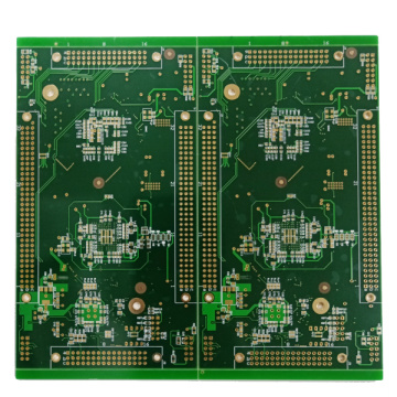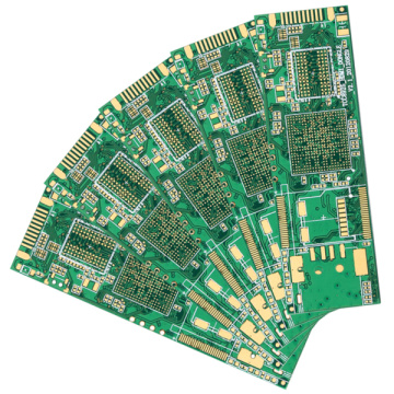
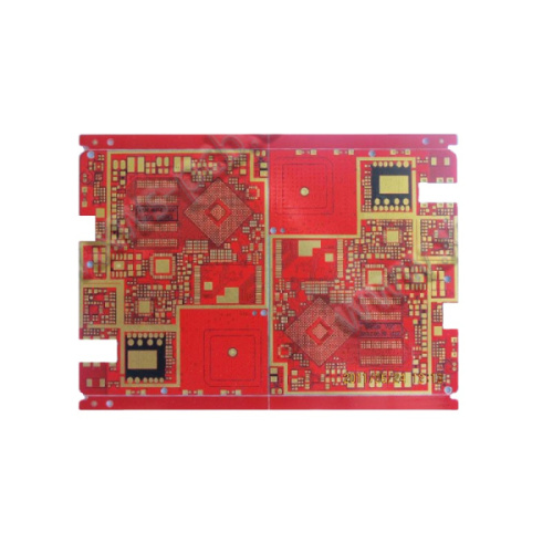
HDI Differential Characteristic impedance PCB
-
$1.98≥1 Piece/Pieces
- Min. Order:
- 1 Piece/Pieces
- Min. Order:
- 1 Piece/Pieces
- Transportation:
- Ocean, Land, Air, Express
- Port:
- shenzhen
Your message must be between 20 to 2000 characters
Contact Now| Supply Ability: | 10000pcs/day |
|---|---|
| Payment Type: | T/T,Paypal |
| Incoterm: | FOB,EXW |
| Transportation: | Ocean,Land,Air,Express |
| Port: | shenzhen |
How do you specify control impedance of PCB?
As the circuit design becomes more complex and high-speed, how to ensure the integrity of various signals (especially the high-speed signal Microwave radio frequency board), that is, to ensure the signal quality, has become a difficult problem. At this time, it is necessary to use transmission line theory for analysis. Controlling the characteristic impedance matching of the signal line becomes the key. The non-strict impedance control of the Characteristic impedance PCB will cause considerable signal reflection and signal distortion, leading to design failure. Common signals, such as PCI bus, PCI-E bus, USB, Ethernet, DDR memory, LVDS signal, etc. Characteristic impedance PCB, all require impedance control. Impedance control ultimately needs to be realized through PCB design, and higher requirements for the characteristic impedance PCB process are also put forward. After communicating with the PCB factory and combining the use of EDA software, I have some superficial understanding of this issue, and I would like to share it with you.
The structure of the multilayer board:
In order to control the impedance of the Characteristic impedance PCB well, we must first understand the structure of the PCB:
Usually, what we call a multilayer board is made by laminating a core board and a prepreg. The core board is a hard, specific thickness, two-bread copper plate, which is the basic material of the printed board. . The prepreg constitutes the so-called wetting layer, which plays the role of bonding the core board. Although it also has a certain initial thickness, its thickness will change during the pressing process.
Usually the two outermost dielectric layers of the multilayer board are both wetting layers, and a separate copper foil layer is used as the outer copper foil on the outside of the two layers. The original thickness specifications of the outer copper foil and inner copper foil are generally 0.5OZ, 1OZ, 2OZ (1OZ is about 35um or 1.4mil), but after a series of surface treatments, the final thickness of the outer copper foil is average It will increase by about 1OZ. The inner copper foil is the copper clad on both sides of the core board, and its final thickness is very small from the original thickness, but due to etching, it is generally reduced by a few um.
The outermost layer of the multilayer board is the solder mask, which is what we often call "green oil". Of course, it can also be yellow or other colors. The thickness of the solder mask is generally not easy to accurately determine. The area without copper foil on the surface is slightly thicker than the area with copper foil. However, because of the lack of copper foil thickness, the copper foil still appears more prominent. When we use You can feel it when your finger touches the surface of the printed board.


Related Keywords