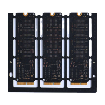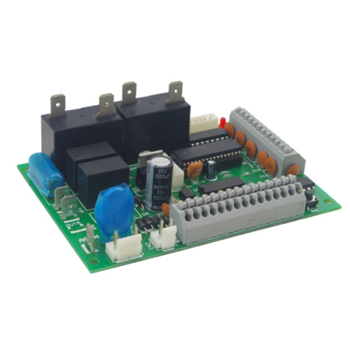


Energy saving heat pump control pcb design
-
$120.00≥1 Piece/Pieces
- Min. Order:
- 1 Piece/Pieces
- Min. Order:
- 1 Piece/Pieces
Your message must be between 20 to 2000 characters
Contact NowHow are PCBs put together?
With the continuous development of the entire electronics industry, many products in the electronics industry have established mature upstream and downstream supporting enterprises. From mature product design, design, manufacturing, assembly testing, packaging, wholesaler channels, etc., such an industrial chain naturally arises in a specific environment. Therefore, the connection between design and manufacturing is very close and in an inseparable position.
One of the most important aspects of electronic products from design completion to manufacture is the processing of PCB boards. Most pcbs are made by Surface-Mount (SMT) &BGA Assembly.
Then the problem came. Now electronic products are developing in the direction of being small and light. When your design PCB board is particularly small, some electronic product modules are as small as a few centimeters square. In terms of PCB Mixed Assembly, it brings problems. There is no way to assemble such a small PCB on the production line!
Here, a small piece of PCB needs to be inlaid together, which is more convenient for the placement machine. Usually, the manufacturer of the circuit board will provide the service of the panel size, but in the design of the Altium Designer software, there are many advantages. as follows:
1. The board of directors can be the direction you want
2. The panel file is associated with the original board, and the original board changes will be automatically updated to the panel
3. You can put several different circuit boards together
How to anel board in Altium Designer?
Here we use an example to introduce the process and operation steps of the panel in Altium Designer.
1. First of all, ensure the size of the circuit board. You can use Reports>Board Information to view this information. As shown in the figure below, the board is used as a PCB board with a size of 75.18 x 30.23mm. We will spell a 2x2 PCB array on a new PCB.


4. After setting the above parameters, click "OK" to place the array board on the PCB. Adjust the position just right. And reposition the origin of the PCB to the origin of the array board.

The figure below shows an array board with detailed traces.

Finally, it converts the PCB array board to process graphics files, such as Gerber. Give the PCB processing board factory and communicate the specific process requirements and details with the circuit board factory.

If any changes are made to the original PCB, these changes can be updated in the PCB template file with one click. For example, in the image below, the pads are placed in the original PCB.
Then in the PCB panel file, click Refresh to refresh, and each of these boards will have such a mat. Update using the original board. As follows.

To put different PCBs together, just select a PCB file and spell out the array. Then select another PCB file and spell out the array. As follows.
It should be noted here that for different PCBs put together, the number of layers and thickness settings of the PCB must be exactly the same.


Related Keywords