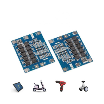


3.7V li-ion Battery Packs PCM BMS PCB PCBA
-
$120.00≥1 Piece/Pieces
- Min. Order:
- 1 Piece/Pieces
- Min. Order:
- 1 Piece/Pieces
Your message must be between 20 to 2000 characters
Contact NowWhat is the purpose of vias?
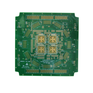
Via is one of the important components of multi-layer PCB, and the cost of drilling usually accounts for 30% to 40% of PCB manufacturing cost. To be more complicated, every hole on the PCB can be called a via. From the point of view of function, vias can be divided into two types: one is used for electrical connection between layers; the other is used for fixing or positioning of Electronic Components and Electronic connectors. As far as the process is concerned, these vias are generally divided into three categories, namely blind via PCB, buried via PCB and through via PCB. Blind holes are located on the outer surface of the top and bottom layers of the printed circuit board and have a certain depth. They are used to connect the surface circuit and the upper inner circuit. The depth of the hole usually does not exceed a certain ratio (aperture). Buried hole refers to the connection hole located in the inner layer of the printed circuit board, which does not extend to the surface of the circuit board. The above two types of holes are located in the inner layer of the circuit board, and the through hole forming process is used before lamination, and several inner layers can be stacked during the process of forming the via hole. The third type is called a through hole, which penetrates the entire circuit board and can be used to complete external interconnection or as a device positioning hole for Electronic Components. Because the through hole is easier to complete in the process and low cost pcb manufacturing, most of the printed circuit boards use it instead of the other two types of through holes. The via holes mentioned below, if not specifically clarified, are considered as via holes.


Second, the parasitic capacitance of the via
The via itself has a parasitic capacitance to the ground. If it is known that the diameter of the isolation hole on the ground layer of the via is D2, the diameter of the via pad is D1, the thickness of the PCB board is T, and the dielectric constant of the board substrate is ε, then the parasitic capacitance of the via is approximately:
C=1.41εTD1/(D2-D1)
The parasitic capacitance of the via will have a secondary effect on the circuit formation, which is to extend the rise time of the signal and reduce the speed of the circuit. For example, for a PCB with a thickness of 50Mil, if a via with an inner diameter of 10Mil and a pad diameter of 20Mil is used, and the distance between the pad and the ground copper area is 32Mil, then we can approximate the via using the following formula The parasitic capacitance is roughly: C=1.41x4.4x0.050x0.020/(0.032-0.020)=0.517pF, the rise time change caused by this part of the capacitance is: T10-90=2.2C(Z0/2)=2.2 x0.517x(55/2)=31.28ps. It can be seen from these values that although the effect of the rise delay caused by the parasitic capacitance of a single via is not very clear, if the via is repeatedly used in the trace to stop the switching between layers, the designer should still consider carefully.
Third, the parasitic inductance of the via.
Similarly, there are parasitic capacitances in vias and parasitic inductances. In the design of high-speed digital circuits, the harm caused by parasitic inductances of vias is often greater than the impact of parasitic capacitance. Its parasitic series inductance will weaken the contribution of the bypass capacitor and weaken the filtering effect of the entire power supply system. We can use the above formula to complexly calculate the parasitic inductance of a via:
L=5.08h[ln(4h/d)+1] where L refers to the inductance of the via, h is the length of the via, and d is the diameter of the center hole. It can be seen from the formula that the diameter of the via has a small influence on the inductance, and the length of the via has the greatest influence on the inductance. Still using the following example, the inductance of the via can be calculated as: L=5.08x0.050[ln(4x0.050/0.010)+1]=1.015nH. If the rise time of the signal is 1ns, then its equivalent impedance is: XL=πL/T10-90=3.19Ω. Such impedance should not be neglected in the presence of high-frequency currents. Special attention should be paid to the fact that the bypass capacitor needs to pass through two vias when connecting the power layer and the ground layer, so that the parasitic inductance of the via will increase exponentially.
After analyzing the parasitic characteristics of vias above, we can see that in high-speed PCB design, the seemingly complex process
Holes often also bring great negative effects to circuit design. In order to reduce the adverse effects caused by the parasitic effects of the vias, the following can be done in the design:
1. From the perspective of cost and signal quality, choose a reasonable size of vias. For example, for the 6-10 layer memory module PCB design, it is better to use 10/20Mil (drilled/pad) vias. For some high-density small-size HDI PCBs, you can also try to use 8/18Mil Via. Under current technical conditions, it is difficult to use smaller vias. Regarding the power or ground vias, you can think about using a larger size to reduce the impedance.
2. The two formulas discussed below can be obtained, and the use of a thinner PCB is beneficial to reduce the two parasitic parameters of the via.
3. Try not to change the layers of the signal traces on the PCB board, that is, try not to use unnecessary vias.
4. The pins of the power supply and the ground should be punched nearby, and the lead between the vias and the pins should be as short as possible, because they will cause the addition of inductance. At the same time, the power and ground leads should be as thick as possible to increase impedance.
5. Place some grounded vias near the vias of the signal layer to provide the nearest loop for the signal. It is even possible to place a small amount of redundant ground vias on the PCB board. Of course, it needs to be sensitive and changeable when designing. The via model discussed later is the condition that each layer has pads. In some cases, we can reduce or even remove the pads of some layers. Especially when the via density is very large, it can cause a broken slot to form a circuit breaker in the copper layer. In addition to moving the position of the via hole, we can also think about placing the via hole on the copper layer. The pad size is reduced.


Related Keywords