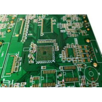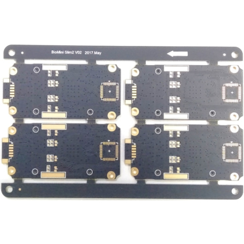
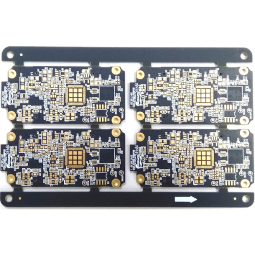
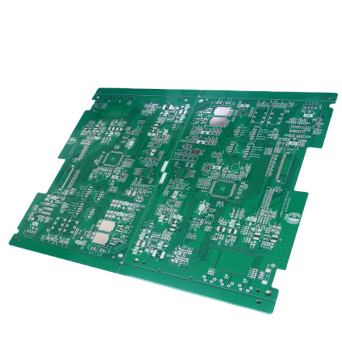
8 Layer Button Motor Controller Circuits pcb
-
$0.89≥3 Piece/Pieces
- Min. Order:
- 3 Piece/Pieces
- Min. Order:
- 3 Piece/Pieces
Your message must be between 20 to 2000 characters
Contact Now
What is the difference between thru hole vias blind vias and buried vias?
How to distinguish between through hole PCB, buried PCB and blind via hole of BVH PCB?
Generally, there are three kinds of guide holes that we often see, namely:
Through Hole: Plating Through Hole, or PTH for short, is the most common type. You only need to pick up the PCB and face the light, and the holes that can see the bright light are "through holes". This is also the simplest type of hole, because you only need to use a drill to make it
Or the laser can directly drill the circuit board, and the cost is relatively cheap. However, some circuit layers do not need to connect these through holes. For example, we have a six-story house. I bought its third and fourth floors. I want to design a staircase inside that only connects the third floor to the third floor. It is fine between the fourth floor. For me, the space on the fourth floor is virtually used up by the original staircase connecting the first floor to the sixth floor. So although through holes are cheap, they sometimes use up more PCB space.
Blind via hole: Blind Via Hole, which connects the outermost circuit of the PCB with the adjacent inner layer with electroplated holes. Because the opposite side cannot be seen, it is called "blind through". In order to increase the space utilization of the PCB circuit layer, a "blind via" process has emerged. This production method is
Need to pay special attention to the depth of the drilling (Z-axis) to be just right, but this method often causes difficulties in plating in the hole, so it is almost used by no manufacturer; it is also possible to drill the circuit layers that need to be connected in advance when the individual circuit layers are drilled. Hole, finally glued together,
However, more precise positioning and alignment devices are required.
Buried hole: Buried hole, the connection of any circuit layer inside the PCB but not conducting to the outer layer. This process cannot be achieved by drilling after bonding. The drilling must be performed on the individual circuit layers. After the inner layer is partially bonded, it must be electroplated.
Finally, it can be fully bonded, which is more labor-intensive than the original "through holes" and "blind holes", so the price is the most expensive. This process usually only uses HDI PCB to increase the usable space of other circuit layers.


Related Keywords