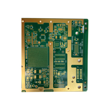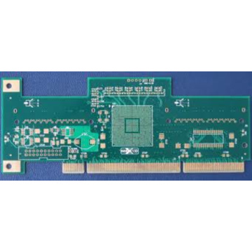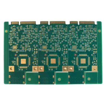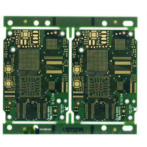


Quick Turn PCB 48 hours 6 layer PCB
-
$0.09≥1 Piece/Pieces
- Min. Order:
- 1 Piece/Pieces
- Min. Order:
- 1 Piece/Pieces
Quantity:
Your message must be between 20 to 2000 characters
Contact NowBasic Info
Basic Info
Product Description
Product Description
What is a buried via?
With the current design of portable products moving towards miniaturization and high density, PCB design is becoming more and more difficult, and higher requirements are put forward for the PCB production process. In most of the current portable products, the Surface-Mount (SMT) & BGA Assembly with a pitch of less than 0.65mm all use the blind and buried via design process, so what is the blind and buried via?
Blind vias (Blind vias / Laser Vias): blind via hole PCB is a type of via that connects the inner traces of the PCB to the traces on the surface of the PCB. This hole does not penetrate the entire board.
Buried vias: The buried PCB only connects the via type of the traces between the inner layers, so it is invisible from the surface of the PCB.
The figure is a schematic diagram of the cross-sectional structure of an 8-layer High frequency board:

A: Through hole (L1-L8)
B: Buried hole (L2-L7)
C: Blind hole (L7-L8)
D: Blind hole (L1-L3)


Related Keywords
Related Keywords
You May Also Like
You May Also Like