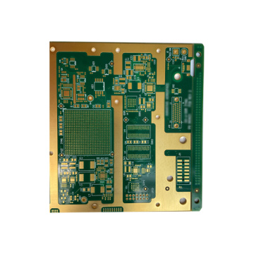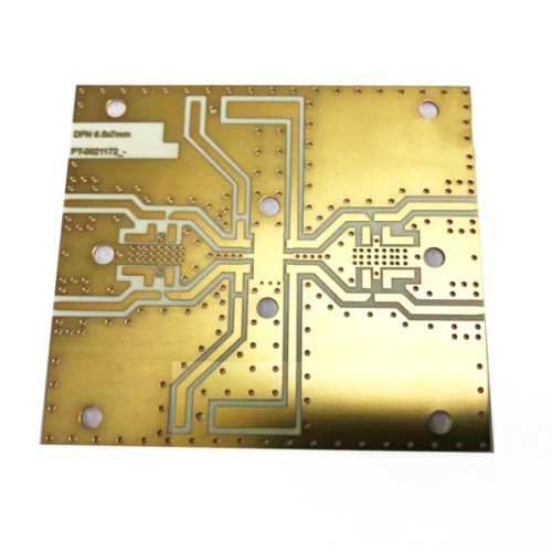
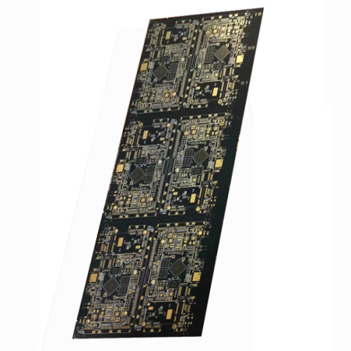


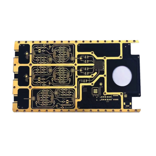
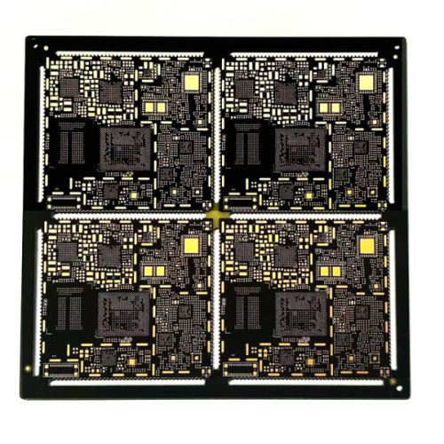
3OZ thick copper SMT circuit assembly pcb pcba
-
$0.09≥1 Piece/Pieces
- Min. Order:
- 1 Piece/Pieces
- Min. Order:
- 1 Piece/Pieces
- Transportation:
- Ocean, Land, Air, Express, Others
Your message must be between 20 to 2000 characters
Contact Now| Payment Type: | T/T,Paypal,Others |
|---|---|
| Incoterm: | FOB,EXW |
| Transportation: | Ocean,Land,Air,Express,Others |
What is plating in PCB?
There are two standard methods for growing metal build-up layers in PCB wires and through holes: circuit electroplating and full-board copper plating, which are described as follows.
1. Line plating
In this process, only the copper layer generation and etching resist metal plating are accepted where the circuit patterns and through holes are designed. During the circuit electroplating process, the increased width of each side of the circuit and the solder pad is roughly equivalent to the increased thickness of the electroplated surface. Therefore, it is necessary to leave a margin on the original film.
In circuit electroplating, most of the copper surface must be masked by resist, and electroplating is only performed where there are circuit patterns such as circuits and solder pads. Since the surface area that needs to be plated is reduced, the required power supply current capacity is usually greatly reduced. In addition, when using contrast reverse photopolymer dry film plating resist (the most commonly used type), the negative film It can be made with a relatively inexpensive laser printer or drawing pen. The copper consumption of the anode in the circuit electroplating is less, and the copper that needs to be removed during the etching process is also less, so the analysis and maintenance costs of the electrolytic cell are reduced. The disadvantage of this technique is that the circuit pattern needs to be plated with tin/lead or an electrophoretic resist material before etching, and it is removed before the solder resist is applied. This adds complexity and adds an additional set of wet chemical solution treatment processes.
2. Copper plating on the whole board
During this process, all surface areas and drill holes are plated with copper, and some resist is poured on the unneeded copper surface, and then an etching resist metal is plated. Even for a medium-sized High Quality Prototype PCB Fabrication, this requires an electrical excavation that can provide a considerable amount of current to make an easy-to-clean, smooth and bright copper surface for subsequent buried PCB and blind via hole PCB processes. use. If you don't have a photoelectric plotter, you need to use a negative film to expose the circuit pattern, making it a more common contrast inversion dry film photoresist. Etching the Quick Turn PCB with copper plating on the entire board will remove most of the material plated on the PCB again. As the copper carrier liquid in the etchant increases, the burden of additional corrosion on the anode is greatly increased.


Related Keywords