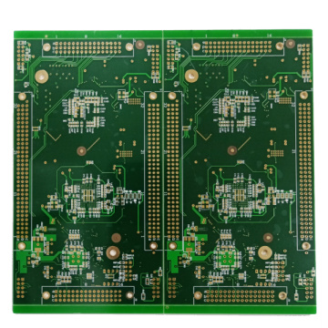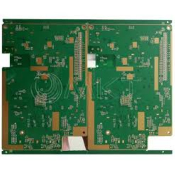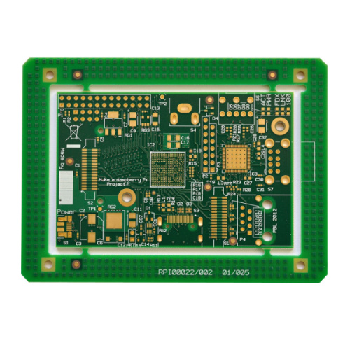


Fast 48 hours HDI High Density Interconnect PCB
-
$0.09≥1 Piece/Pieces
- Min. Order:
- 1 Piece/Pieces
- Min. Order:
- 1 Piece/Pieces
- Transportation:
- Ocean, Land, Air, Express, Others
- Port:
- shenzhen
Your message must be between 20 to 2000 characters
Contact Now| Supply Ability: | 10000pcs/day |
|---|---|
| Payment Type: | T/T,Paypal,Others |
| Incoterm: | FOB,EXW |
| HS Code: | 853400 |
| Transportation: | Ocean,Land,Air,Express,Others |
| Port: | shenzhen |
What is HDI High Density Interconnect?
High-density interconnection (HDI) PCB is a technology of custom pcb fabrication. It is a BVH PCB with a relatively high line distribution density using micro-blind via and buried via technology, buried PCBt blind via hole PCB. With the continuous development of technology, in order to meet the electrical requirements of high-speed signals, PCBs must provide impedance control with AC characteristics, high-frequency transmission capabilities, and reduction of unnecessary radiation (EMI). Sometimes in order to reduce the quality of signal transmission, insulating materials with low dielectric coefficient and low attenuation are generally used. In order to better match the miniaturization and arraying of Electronic Components and Surface-Mount (SMT) & BGA Assembly, PCBs are constantly increasing their density to meet compliance requirements.
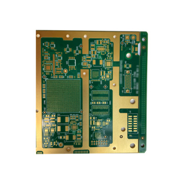
HDI High Quality PCB Products include laser blind vias and mechanical blind vias; in order to achieve the technology of conduction between the inner and outer layers, generally through and buried vias, blind vias, stacked vias, staggered vias, cross blind buried, through holes, and blind hole filling Hole electroplating, fine lines and small gaps, micro-holes in the disk and other processes to achieve.
HDI circuit boards can be divided into: 1st order, 2nd order, 3rd order, 4th order and any layer interconnection
1st order HDI structure: 1+N+1 (2 times of pressing, 1 time of laser)
2nd order HDI structure: 2+N+2 (pressing 3 times, laser 2 times)
3-level HDI structure: 3+N+3 (4 times of pressing, 3 times of laser)
4-level HDI structure: 4+N+4 (5 times of pressing, 4 times of laser)
From the above structure, it can be concluded that the laser shot once is a 1-step board, twice is a 2-step board, and so on.
At present, the HDI circuit boards that can be used in batches for Shenze multilayer circuits are mainly within the 3rd order, and the 4th order and any layer interconnection is limited to small batch sample production. At present, we are intensifying research and development. I believe that the 4th order HDI High Quality PCB will be in the near future. Products and any layer interconnection will be mass-produced.


Related Keywords