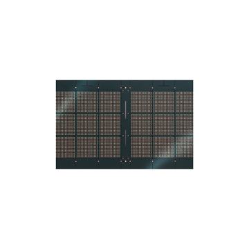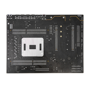

4-Layer Multilayer PCB with Immersion Gold Surface
-
$10.00≥1 Piece/Pieces
- Min. Order:
- 1 Piece/Pieces
- Min. Order:
- 1 Piece/Pieces
- Transportation:
- Ocean, Land, Air
- Port:
- Shenzhen
Quantity:
Your message must be between 20 to 2000 characters
Contact NowBasic Info
Basic Info
| Payment Type: | Paypal,T/T |
|---|---|
| Incoterm: | FOB,EXW |
| Transportation: | Ocean,Land,Air |
| Port: | Shenzhen |
Product Description
Product Description
Steps involved in the PCB assembly processThere are many steps involved in the PCBA and manufacturing process. To get the best quality final product, follow these steps:
Step 1: Add Solder Paste: This is the very initial stage of the assembly process. At this stage, solder paste is added to the component pads wherever soldering is required. Put the solder paste on the pads and stick it in the right place with the help of the solder screen. This screen is made from a PCB file with holes. Step 2: Placing Components: With the solder paste added to the component pads, it's time to place the components. The PCB goes through a machine that precisely places these components on the pads. The tension provided by the solder paste holds the component in place. Step 3: Reflow Oven: This step is used to permanently attach the components to the board. After the components are placed on the board, the PCB is passed through the reflow oven conveyor. The controlled heat of the oven melts the solder added in the first step, permanently connecting the components.Step 4: Wave Soldering: In this step, the PCB is passed through a wave of molten solder. This will create an electrical connection between the solder, the PCB pads and the component leads. Step 5: Cleaning: At this step, all the soldering process is completed. During the soldering process, a large amount of flux residue forms around the solder joint. As the name suggests, this step involves cleaning flux residues. Clean flux residue with deionized water and solvent. With this step, the PCB assembly is completed. Subsequent steps will ensure that the assembly is done correctly. Step 6: Testing: At this stage, the PCB assembly is complete and inspections begin to test the placement of the components. This can be performed in two ways: l Manual: This inspection is usually carried out for smaller components, the number of components does not exceed one hundred. l Automatic: This check is performed to check for bad joints, wrong components, misplaced components, etc.


Related Keywords
Related Keywords
You May Also Like
You May Also Like