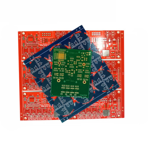
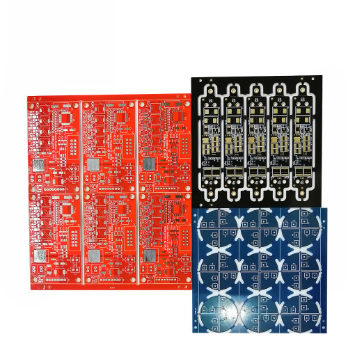
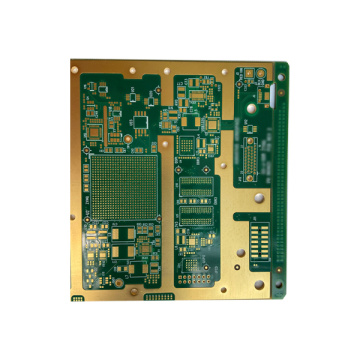
PCB Fabrication, Shenzhen PCB High demand PCB,
- Min. Order:
- 1 Piece/Pieces
- Min. Order:
- 1 Piece/Pieces
Quantity:
Your message must be between 20 to 2000 characters
Contact NowBasic Info
Basic Info
Product Description
Product Description
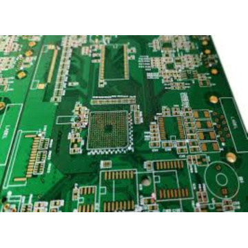
What are 2-layer and 4-layer PCBs?
What is the difference between a four-layer PCB and a two-layer PCB? First, let us briefly understand what is a four-layer PCB? What is a double-sided PCB?


In order to increase the wiring area of the four-layer PCB, more single-sided or double-sided wiring PCBs are used. The four-layer PCB uses two double-layer PCBs, and an insulating layer is placed between each layer of PCB and then bonded (press-fitted). The number of PCB layers represents several independent wiring layers, usually an even number, including the two outermost layers. A four-layer PCB can be called a multi-layer PCB, and the difference between a multi-layer PCB and a double-sided PCB is big.

First of all, in terms of the number of layers, a four-layer PCB has more layers than a double-sided PCB. Therefore, the four-layer PCB needs to be pressed on the basis of the double-sided PCB when it is made. When pressing, PP and copper foil are added to both sides of the double-sided PCB to form a four-layer PCB at high temperature and high pressure. Simply put, a four-layer PCB has an inner layer, and the inner layer needs to be etched during production, and then pressed and pressed after the etching, while the double-sided PCB can directly cut the sent PCB material and then drill.
Four-layer PCB refers to a PCB made of four-layer glass fiber for circuit printing, which can reduce the cost of the PCB, but the efficiency is poor.
PCB
Although a four-layer PCB can be seen by observing the cut surface of the PCB, this method is actually more difficult, and few people have this kind of vision. But the four-layer PCB can be quickly identified by observing the via hole. If the same guide holes can be found on both sides of the PCB, or the main PCB or display card is aligned with the light source, if the position of the guide holes cannot transmit light, it is a four-layer PCB.
In short, the four-layer PCB has more layers than the double-layer PCB, and there will be more steps in the production process. The four-layer PCB has an inner layer, which needs to be etched on the inner layer, and then pressed and pressed after the etching, while the double-sided PCB does not need to cut and drill the PCB material directly.


Related Keywords
Related Keywords
You May Also Like
You May Also Like