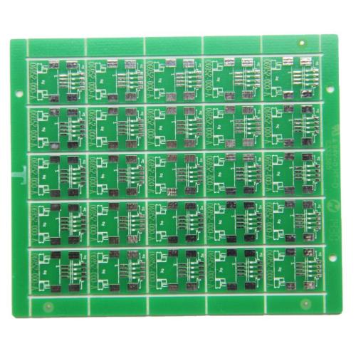
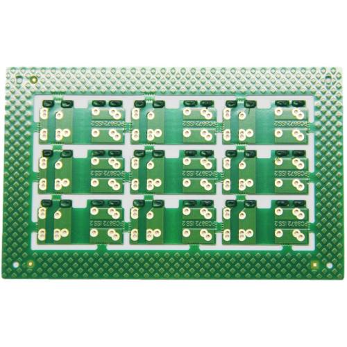
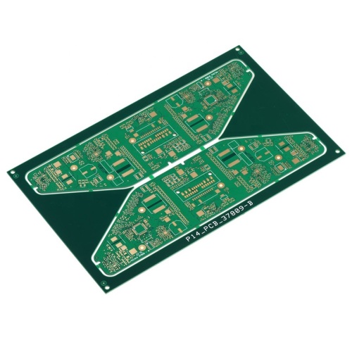
low cost for high volume batches PCB
-
$0.10≥1 Piece/Pieces
- Min. Order:
- 1 Piece/Pieces
- Min. Order:
- 1 Piece/Pieces
- Transportation:
- Ocean, Land, Air, Express
- Port:
- SHENZHEN
Your message must be between 20 to 2000 characters
Contact Now| Place of Origin: | SHENZHEN |
|---|---|
| Productivity: | 20000sqm/month |
| Supply Ability: | 20000sqm/month |
| Payment Type: | L/C,T/T,Paypal,Others |
| Incoterm: | FOB,Express Delivery,EXW |
| Certificate: | ISO/UL |
| HS Code: | 85340090 |
| Transportation: | Ocean,Land,Air,Express |
| Port: | SHENZHEN |
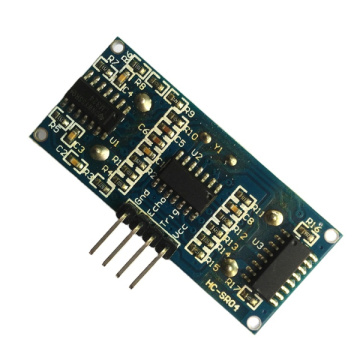
What is ENIG PCB?
The full name of ENIG is Electroless Nickel Immersion Gold.
The purpose of the gold-immersion process is to deposit a nickel-gold coating with stable color, good brightness, flat coating, and good solderability on the surface of the printed circuit. Basically, it can be divided into four stages: pre-treatment (degreasing, micro-etching, activation, post-dipping), immersion of nickel, immersion of gold, and post-treatment (washing waste gold with water, washing with DI water, and drying). When you need to make a button printed circuit board or custom keyboard pcb, you may need to sink gold, the board of sinking gold is not easy to rust, and the contact resistance is small and it would be easier on PCBA process.The surface of ENIG would be smoother than HASL so when it would be easier to bone with components after SMT andThrough-Hole Assembly process.


Related Keywords