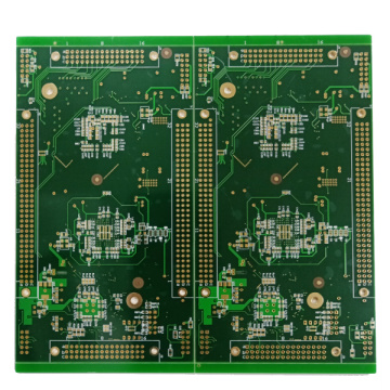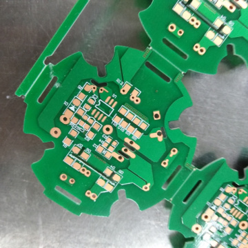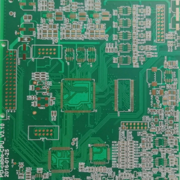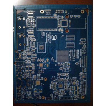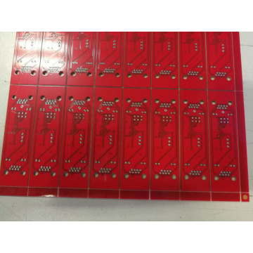
Double Side PCB, double layer PCB and 2 Layers PCB
-
$0.72≥1 Piece/Pieces
- Min. Order:
- 1 Piece/Pieces
- Min. Order:
- 1 Piece/Pieces
- Transportation:
- Express, Air, Ocean
- Port:
- Shenzhen
Your message must be between 20 to 2000 characters
Contact Now| Payment Type: | T/T,Paypal |
|---|---|
| Incoterm: | FOB,EXW |
| Transportation: | Express,Air,Ocean |
| Port: | Shenzhen |
How does PCB assembly work?
PCBA manufacturing process involve many steps. If you want to obtain the best quality final product, follow these steps:
Step 1: Add solder paste: This is the initial stage of the assembly process. At this stage, solder paste is added to the component pads wherever soldering is required. Put the solder paste on the pad and paste it in the correct position with the help of the soldering screen. This screen is made of PCB files and has holes and Through-Hole Assembly.
Step 2: Place the component: After adding the solder paste to the component pad, it is time to place the component. The PCB passes through a machine that precisely places these components on the pads. The tension provided by the solder paste holds the components in place.
Step 3: Reflow oven: This step is used to permanently fix the components on the board. After placing the components on the board, the PCB passes through the reflow oven conveyor belt. The controlled heat of the oven melts the solder added in the first step, thereby permanently connecting the components.
Step 4: Wave soldering: In this step, the PCB is passed through a wave of molten solder. This will establish electrical connections between the solder, PCB pads and component leads ,Surface-Mount (SMT) &BGA Assembly
Step 5: Cleaning: Up to this step, all welding processes have been completed. During the soldering process, a large amount of flux residue will form around the solder joints. As the name suggests, this step involves cleaning flux residues. Clean the flux residue with deionized water and solvent. Through this step, PCB assembly is completed. The next steps will ensure that the assembly is completed correctly.
Step 6: Testing: At this stage, the Mixed Assembly is completed and inspections are started to test the position of the components. This can be performed in two ways:


Related Keywords