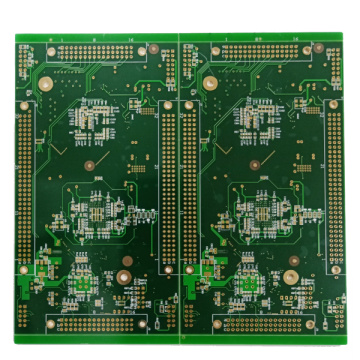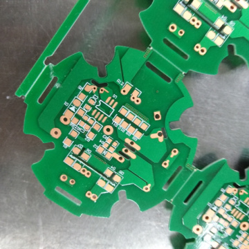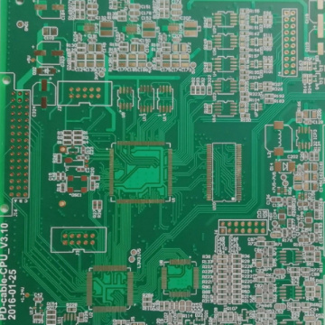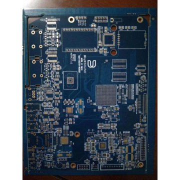
4 Layer pcb manufacturing pcba prototype cheap price
-
$0.10≥5 Piece/Pieces
- Min. Order:
- 5 Piece/Pieces
- Min. Order:
- 5 Piece/Pieces
- Transportation:
- Ocean, Land, Air, Express, Others
- Port:
- Shenzhen
Your message must be between 20 to 2000 characters
Contact Now| Supply Ability: | 10000 square meters/month |
|---|---|
| Payment Type: | T/T |
| Incoterm: | FOB,EXW |
| Transportation: | Ocean,Land,Air,Express,Others |
| Port: | Shenzhen |
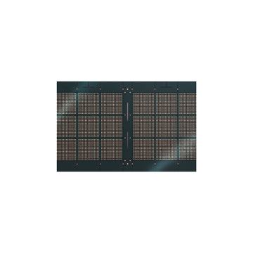
What is 4 layer PCB?
Printed Circuit boards are Printed with four layers of glass fiber, which can reduce the cost of PCB but is not very efficient.
Then four layers, double panels, single panels, 6 layers, etc. How to distinguish, the following introduction to distinguish the number of PCB layers:
(1) by watching the section of the PCB board, in fact, this method is more difficult, few people have this vision.
(2) by observing the guide hole can be identified.
If the same guide holes can be found on both sides of the PCB board, or the main board or display card is facing the light source, if the position of the guide holes is not transparent, it is a four-layer board low cost 4 layer pcb supplier.
Four layer board copy board method
The four-layer board copy is a PCB board whose components have been removed and its surface is clean. We need to copy it into a PCB file, and follow the following steps:
1. Scan the top panel, save the picture and name it top.jpg. At this time, set the scanning DPI according to the density, if set to 400DPI.
2. Scan the bottom plate, save the image and name it Bottom.jpg
3. Grinding the middle layer 1 with coarse sandpaper to leak out the copper skin, scanning the image after cleaning, and naming it as MID1.jpg
4. Grinding the middle layer 2 with coarse sandpaper, leaking out the copper skin, scanning the image after cleaning, and naming it as MID2.jpg
5. In Photoshop, adjust each image horizontally (select the image to ensure that the picture is horizontal, so that the line out of the good, and the multiple images are easy to align up and down). It is recommended that the bottom image be mirrored horizontally, so that the top and bottom images are in the same direction, and the upper and lower positioning holes are consistent.
Finally, save each image into a BMP file, such as top.bmp, bottom.bmp, mid1.bmp, mid2.bmp.
Note here do not need to crop the picture exactly, it is best to leave some rich, basically as long as the picture level is done.
6, Open the Color Copy software, from the main menu "File" - >;
"Open BMP file ", select top. BMP file to open Heavy copper board.
7, after setting the DPI, you can copy the top layer map, first choose the layer to the top, and then start to put components, through holes, wires, etc.
8. After putting everything in the top layer, save the temporary file (both in the manual and help, you can choose it by yourself through the menu or the button in the toolbar) and name it Top-1. DPB (it is suggested to name the names saved at different times in the middle with different numbersQuickturn PCBs with 2 day.
Top -1. DPB,top-2. DPB,top- 1. DPB,top-2. DPB,top- 1. DPB,top-2. DPB,top- 1. DPB,top-2. DPB,top- 1.
9. Close the current picture window (note that only one picture can be opened at a time, never open more than one picture).
10. From the main menu "File" - >
"Open BMP file ", select bottom. BMP, and then open the temporary file Top-1.dpb. At this time, you will find that the drawing on the top level is not aligned with the background drawing on the bottom level.
Select a few reference points and the background map corresponding points aligned, then you can choose the current layer as the bottom, open is to walk the bottom line, pad, fill, etc., if the top line blocking the bottom, what to do?Low Cost Prototype PCB
Very simple, you can select "Layer Color Settings" from the main menu "Options", click off the top layer, and the top layer screen printing can also be turned off.
After copying the bottom layer, save the temporary file as bottom-1.dpb, or save the PCB file as bottom-1.pcb. The file will now be a two-layer aligned file.One stop BOM purchase Solution
11. Similarly, the board reading process of the middle layer is the same. Repeat steps 9~10, and the final output PCB file is the four layers of PCB map put together, which is exactly the same as the real object.


Related Keywords