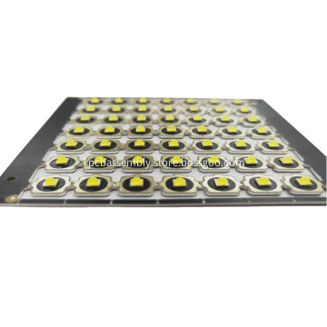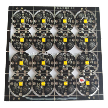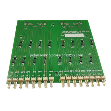


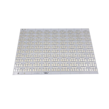
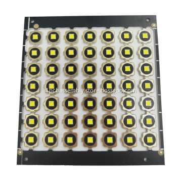
Custom bluetooth speaker pcb assembly pcb pcba
- Payment Type:
- T/T, Paypal, Money Gram, Western Union
- Incoterm:
- FOB, CFR, CIF
- Min. Order:
- 1 Piece/Pieces
- Min. Order:
- 1 Piece/Pieces
- Delivery Time:
- 5-30 Days
- Transportation:
- Ocean, Land, Air, TNT
- Port:
- Shenzhen, HongKong
Your message must be between 20 to 2000 characters
Contact Now| Place of Origin: | Shenzhen China |
|---|---|
| Productivity: | 500,000pcs per Month |
| Supply Ability: | 500,000pcs per Month |
| Payment Type: | T/T,Paypal,Money Gram,Western Union |
| Incoterm: | FOB,CFR,CIF |
| Certificate: | ISO9001, IATF16949, IPC-A-610F |
| HS Code: | 8517709000 |
| Transportation: | Ocean,Land,Air, TNT |
| Port: | Shenzhen,HongKong |
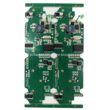
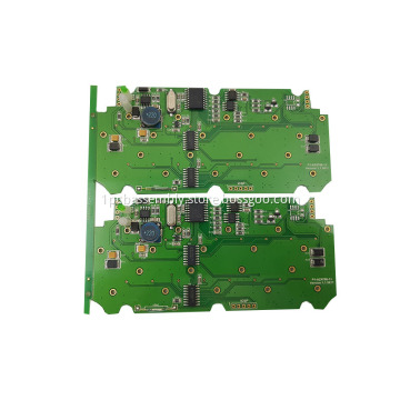
Custom bluetooth speaker pcb assembly pcb pcba
Subtractive methods remove copper from an entirely copper-coated board to leave only the desired copper pattern. In additive methods the pattern is electroplated onto a bare substrate using a complex process. The advantage of the additive method is that less material is needed and less waste is produced. In the full additive process the bare laminate is covered with a photosensitive film which is imaged (exposed to light through a mask and then developed which removes the unexposed film). The exposed areas are sensitized in a chemical bath, usually containing palladium and similar to that used for through hole plating which makes the exposed area capable of bonding metal ions. The laminate is then plated with copper in the sensitized areas. When the mask is stripped, the PCB is finished.
Semi-additive is the most common process: The unpatterned board has a thin layer of copper already on it. A reverse mask is then applied. (Unlike a subtractive process mask, this mask exposes those parts of the substrate that will eventually become the traces.) Additional copper is then plated onto the board in the unmasked areas; copper may be plated to any desired weight. Tin-lead or other surface platings are then applied. The mask is stripped away and a brief etching step removes the now-exposed bare original copper laminate from the board, isolating the individual traces. Some single-sided boards which have plated-through holes are made in this way. General Electric made consumer radio sets in the late 1960s using additive boards.
Multi-layer printed circuit boards have trace layers inside the board. This is achieved by laminating a stack of materials in a press by applying pressure and heat for a period of time. This results in an inseparable one piece product. For example, a four-layer PCB can be fabricated by starting from a two-sided copper-clad laminate, etch the circuitry on both sides, then laminate to the top and bottom pre-preg and copper foil. It is then drilled, plated, and etched again to get traces on top and bottom layers.[33]

Our Services:
1. PCB Design: One-stop EMS manufacturer, speciallized in designing wireless charging PCBA, bluetooth earphone & Voice box PCBA and other consumer electronics products.
2. PCB Manufacture: Standard FR4 1-36layer PCB, Flex PCB, Rigid-Flex PCB, HDI PCB, Rogers PCB, Metal Core PCB, etc.
3. PCB Assembly: SMT and THT assembly, available for 01005, fine pitch and BGA assembly.
4. Components Sourcing: Available to source all components shown in BOM file (BOM Kitting), hard to find components and long lead time components, etc.
5. One-Stop Turnkey PCBA Manufacture: PCB design+PCB Manufacture+Components Sourcing+PCB Assembly+Electronic Assembly, or PCB Manufacture+Components sourcing+PCB Assembly, etc.
Technical Capabilities:
|
PCB Manufacture Capabilities |
|
|
Layers |
1-36 layers |
|
Material |
FR-4 (Standard FR4, Mid-Tg FR4, Hi-Tg FR4, Lead free assembly material) , Polymide, Metal Core, Rogers, etc. |
|
Board Thickness |
0.1mm-6.0mm (.016"-.126") |
|
Copper Thickness |
1/2oz-6oz(18um-210um) |
|
Board size |
600mm*1200mm |
|
Min Tracing/Spacing |
0.075mm/0.075mm (3mil/3mil) |
|
Min drilling Hole diameter |
0.15mm(6mil), 0.1mm(4mil)-laser drill |
|
Solder Mask |
LPI, different colors(Green, Green matt, Black, Black Matt, White, Red, Yellow, Blue) |
|
Silkscreen color |
White, Blue, Black, Red, Yellow |
|
Surface finish |
Lead free HASL, immersion gold, golden finger, immersion tin, immersion silver, OSP, Carbon oil, plated hard gold(up to 100u") |
|
Impedance tolerance |
+/-5%~+/-10% |
|
Chamfer of Gold Fingers |
20, 30, 45, 60 |
|
Test |
Flying probe or Testing fixture |
|
PCB Assembly Capabilities |
|
|
Quantity |
From prototype to big volume, no MOQ |
|
Assembly type |
SMT, THT or Hybrid |
|
Parts procurement |
Full turnkey (we provided all components) |
|
Partial turnkey ( Customer provide the main components and we provide the rest) |
|
|
Kitted (Customer provide all components) |
|
|
Component types |
SMT 01005, BGA 0.3mm pitch, QFP 0.3mm pitch, etc. |
|
Test |
Custom testing, ICT, FCT, AOI, Test jig |
Our Team and Office:

Our PCB Manufacture Factory:

Our PCB Assembly Factory:

FAQ:
Q: What files need for custom PCB manufacture?
A: Gerber or .pcb or .pcbdoc or .brd file is required.
Q: What files need for custom PCB assembly order?
A: Gerber and the BOM files are required, if you have pick&place file, send it to us as well.
Q: What is payment terms acceptable?
A: For new customer and the total amount within 10000usd, 100% payment in advance by PayPal or T/T or WU. For total amount beyond 10000usd, please contact us.
Q: What files need for PCB/PCBA clone services?
A: For PCB/PCBA clone service, send us the pictures for evaluate first, and we will need 1-2 samples of the PCB/PCBA board for copying.
Related Keywords