

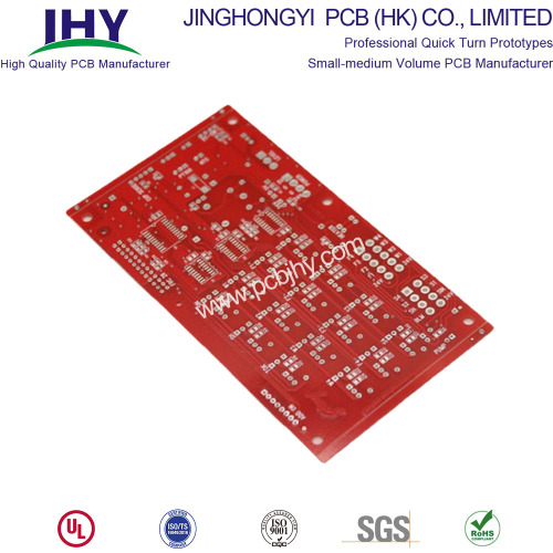

High Tg 170 FR4 8-Layer Impedance Control PCB
- Payment Type:
- L/C, T/T, D/P, Paypal, Money Gram, Western Union
- Incoterm:
- FOB, CFR, CIF, EXW, FCA, CPT, CIP
- Min. Order:
- 1 Piece/Pieces
- Min. Order:
- 1 Piece/Pieces
- Transportation:
- Ocean, Air
Your message must be between 20 to 2000 characters
Contact Now| Place of Origin: | China |
|---|---|
| Productivity: | 10000 |
| Payment Type: | L/C,T/T,D/P,Paypal,Money Gram,Western Union |
| Incoterm: | FOB,CFR,CIF,EXW,FCA,CPT,CIP |
| Certificate: | ISO9001 |
| Transportation: | Ocean,Air |
Keywords: Quality Impedance Control PCB, 8 Layer Impedance Control PCB, High Tg 170 Impedance Control PCB
Production process requirements
Material: FR4, TG170
Layer: 8 Layer
Thickness: 1.6MM
Solder Mask: Red
Silkscreen: White
Surface Treatment: HASL
Certification: UL, ISO 9001, ISO 14001
Minimum Order Quantity: 1 Piece
Packaging Details: vacum packing

High Tg 170 FR4 8-Layer Impedance Control PCB
TG is the maximum temperature (℃) at which the PCB substrate maintains rigidity. Under the high temperature, the common PCB substrate materials continuously produce softening, deformation, melting and other phenomena. At the same time, it also shows in the sharp decline of mechanical and electrical characteristics, which affects the service life of the products. Generally, the temperature of TG is over 130 ℃, the temperature of high Tg is over 170 ℃, the temperature of medium TG is over 150 ℃; generally, the PCB PCB with TG ≥ 170 ℃ is called high Tg PCB. The Tg of PCB is improved, and the heat resistance, moisture resistance, chemical resistance, stability resistance and other characteristics of PCB will be improved. The higher Tg value is, the better the temperature resistance of PCB is. Especially in the lead-free process, high Tg is widely used; high Tg refers to high heat resistance. With the rapid development of the electronic industry, especially the electronic products represented by computers, towards the development of high functionality and multi-layer, higher heat resistance of PCB substrate material is required as the premise. With the emergence and development of high-density installation technology represented by SMT and CMT, PCB can not be separated from the support of high heat resistance of substrate in small aperture, fine circuit, and thin type.
At high temperatures, combustion is also very easy to occur. Therefore, fire prevention has become a problem that must be solved. At this time, we usually think of using PCB board with higher fire rating, which is FR4. FR-4 is a code of fire-resistant material grade, which means that the resin material must be able to extinguish itself after burning. It is not a material name, but a material grade. Therefore, there are many kinds of FR-4 grade materials used in general circuit boards, but most of them are so-called Tera function epoxy resin Plus fillers and fiberglass composites.
Multilayer PCB Impedance Control PCB Manufacturer
With the continuous improvement of electronic technology, more and more traditional circuit board manufacturing methods are far from meeting this high-speed development era. It is undoubtedly the biggest challenge for circuit design engineers to produce PCB with high precision, good performance and cost-saving.
Multilayer PCB (such as 8 layer PCB): when high-precision electronic products are widely used, the circuit can be arranged into a multi-layer structure and pressed together, and through-hole circuits are built between layers to connect the circuits of each layer. Multilayer PCB is the product of high speed, multi-function, large capacity, small volume, thin and lightweight development of electronic product information technology.
Because of the increase of circuits in the multilayer PCB circuit board, the signal interference between circuits becomes a big problem. If there is no impedance control, it will cause considerable signal reflection and signal distortion, leading to design failure. Common signals, such as PCI bus, PCI-E bus, USB, Ethernet, DDR memory, LVDS signal, etc., all need impedance control. Finally, impedance control needs to be realized through PCB design, which also puts forward higher requirements for PCB technology. After communication with PCB Factory, and combined with the use of EDA software, the impedance of wiring is controlled according to the requirements of signal integrity.
The manufacturing difficulty of the multi-layer impedance circuit board increases, and the manufacturing technology and level of PCB manufacturers also need to be improved, which is a problem for general PCB manufacturers. Jinghongyi PCB has been engaged in the production of rigid PCB, flexible PCB, multi-layer PCB, and multi-layer impedance control PCB for nearly 10 years. It has accumulated a lot of production experience, and a group of engineers with professional quality and skilled technical workers can provide more professional production, better service, faster delivery speed, and higher quality products. On the other hand, by improving the production process and process, minimize the impact on the environment and effective cost control, so that customers really enjoy the PCB products with reasonable price and excellent quality.
PCB Impedance Control Meaning and Influence Factor
With the increasing speed of PCB signal switching, PCB designers need to understand and control the impedance of PCB trace. Corresponding to the short signal transmission time and high clock rate of modern digital circuit, PCB trace is no longer a simple connection, but a transmission line.
The impedance value can be obtained by calculation in different ways.
In practice, it is necessary to control the trace impedance when the digital marginal velocity is higher than 1 ns or the analog frequency is higher than 300 MHz. One of the key parameters of PCB trace is its characteristic impedance (that is, the ratio of voltage and current when the wave is transmitted along the signal transmission line). The characteristic impedance of conductor on PCB is an important index of PCB design, especially in the PCB design of the high-frequency circuit, it must be considered whether the characteristic impedance of conductor is consistent with that required by device or signal and whether it matches. This involves two concepts: impedance control and impedance matching
What is Impedance Control in PCB
In order to improve the transmission rate, we must increase the frequency. If the circuit itself is etched, laminated thickness, wire width, and other different factors, it will cause the impedance value change and the signal distortion. Therefore, the impedance value of the conductor on the high-speed circuit board should be controlled within a certain range, which is called "impedance control".The impedance of PCB trace will be determined by its inductive and capacitive inductance, resistance and conductivity. The main factors that affect the impedance of PCB wiring are the width of copper wire, the thickness of copper wire, the dielectric constant of the medium, the thickness of the medium, the thickness of the pad, the path of ground wire, the wiring around the wiring, etc. The PCB impedance range is 25 to 120 ohms.
Characteristic impedance: in practice, the PCB transmission line is usually composed of one conductor trace, one or more reference layers and insulating materials. Traces and layers form the control impedance. PCB will often adopt a multi-layer structure, and the control impedance can also be constructed in various ways. However, regardless of the method used, the impedance value will be determined by its physical structure and the electronic characteristics of the insulating material:
- Width and thickness of the signal trace
- Height of core or pre-filled material on both sides of trace
- Trace and layer configuration
- Insulation constant of core and pre-filled material
The characteristic impedance is also called single line impedance. As the name implies, the impedance of a single wire between control elements is usually 40ohm-60ohm, with 50ohm being the most common.
Differential impedance: the resistance interference between two adjacent signal lines in the same layer. The impedance value is usually 80ohm-120ohm, 90ohm and 100ohm are the most common.
PCB transmission line and lamination
There are two main types of PCB transmission line: microstrip line and stripline line.Microstrip line
The microstrip line is a stripped wire, which refers to the transmission line with only one side of the reference plane, the top and side are exposed to the air (or coated layer), which is located on the surface of Er circuit board with insulation constant, with power supply or ground plane as reference.In the middle is the dielectric. If the dielectric constant, the width of the line and the distance from the ground plane of the dielectric are controllable, its characteristic impedance is controllable, and its accuracy will be within ± 5%.
Stripline line
The stripline is a copper strip placed between two conductive planes. If the thickness and width of the line, the dielectric constant of the medium, and the distance between the two grounding planes are all controllable, the characteristic impedance of the line is also controllable, and the accuracy is within 10%.Difference between microstrip line and stripline line
1. The transmission delay time of a unit length microstrip line is only dependent on the dielectric constant and independent of the width or spacing of the line.2. Because one side of the microstrip line is FR4 (or other dielectric) and the other side is air (low dielectric constant), the speed is very fast, which is conducive to the signal with high-speed requirements (such as differential line, usually high-speed signal, and strong anti-interference).
3. Both sides of the stripline have a power supply or bottom layer, so the impedance is easy to control, and the shielding is better, but the signal speed is slower.
4. Generally, under the same dielectric condition, the loss of microstrip is small (linewidth), and the loss of stripline is large (the line is thin, with vias).
Precautions in Impedance Control PCB laminated design
(1) warpageThe laminated design of PCB should keep symmetry, that is, the thickness of the media layer and copper laying thickness of each layer should be symmetrical up and down. For a six-layer board, it means that the media thickness and copper thickness of top-gnd and bottom-power are the same, and the media thickness and copper thickness of gnd-l2 and l3-power are the same. In this way, the warpage will not occur during lamination.
(2) The signal layer shall be closely coupled with the adjacent reference plane (i.e. the thickness of the medium between the signal layer and the adjacent copper coating shall be very small); the power copper coating and the ground copper coating shall be closely coupled.
(3)In the case of very high speed, extra layers can be added to isolate the signal layer, but it is not recommended to add more power layers to isolate, which may cause unnecessary noise interference.
(4)The typical design layer distribution is shown in the table below:

(5)General principles of layer arrangement:
The lower part (the second layer) of the component surface is the ground plane, which provides the device shielding layer and the reference plane for the top layer wiring; all signal layers shall be adjacent to the ground plane as far as possible; two signal layers shall be avoided to be directly adjacent as far as possible; the main power supply shall be adjacent to the ground plane as far as possible; the lamination structure shall be considered.
Structure of Multilayer PCB
To control the impedance of PCB well, we should first understand the structure of PCB:Generally speaking, the multilayer printed circuit board is composed of core board and semi curing sheets, which is laminated with each other. The core board is a kind of hardboard with specific thickness and two layers of copper, which is the basic material of the printed circuit board. While the semi-cured sheet forms the so-called wetting layer, which plays the role of bonding the core plate. Although it also has a certain initial thickness, its thickness will change during the pressing process.
Generally, the two outermost dielectric layers of the multilayer circuit board are all infiltrating layers, and a separate copper foil layer is used as the outer copper foil. The original thickness specifications of outer copper foil and inner copper foil are generally 0.5oz, 1oz, 2oz (1oz is about 35um or 1.4mil), but after a series of surface treatments, the final thickness of the outer copper foil will increase by about 1oz. The inner copper foil is the copper-clad on both sides of the core plate. The difference between the final thickness and the original thickness is very small. However, due to the reason of etching, it will generally reduce several um.
The outermost layer of the multilayer PCB board is the solder mask layer, which is often called "green oil". Of course, it can also be yellow or other colors. Generally, the thickness of the solder mask layer is not easy to determine accurately. The area without copper foil on the surface is slightly thicker than the area with copper foil. However, due to the lack of the thickness of copper foil, the copper foil is still more prominent, which can be felt when we touch the surface of the PCB with our fingers.
When making PCB of a certain thickness, on the one hand, it is required to select the parameters of various materials reasonably, on the other hand, the final forming thickness of the semi-cured sheet will be smaller than the initial thickness.
Here is a typical 6-layer PCB laminated structure:

PCB Impedance Control Calculator
When we understand the structure of Multilayer PCB and master the required parameters, we can calculate the impedance through EDA software. You can use Allegro to calculate, or you can use polar's cits25, but here we recommend another tool, polarsi9000, which is a good tool for calculating characteristic impedance. Now many PCB factories are using this software.When calculating the characteristic impedance of inner layer signal, whether it is a differential line or single terminal line, you will find that there is only a small gap between the calculation result of polar si9000 and Allegro, which is related to some details, such as the shape of the cross-section of the conductor. But if it is to calculate the characteristic impedance of surface signal, I suggest you choose the coated model instead of the surface model, because this kind of model considers the existence of solder mask, so the result will be more accurate.
Because the thickness of the resistance layer is not easy to control, according to our many years of production experience, an approximate method can be used: subtract a specific value from the calculated results of the surface model, and it is recommended to subtract 8 ohms from the differential impedance and 2 ohms from the single end impedance.
Related Keywords
-
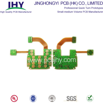
Rigid Flexible Printed Circuit Board
Metal Core Aluminum PCB Single Side PCB manufacturing
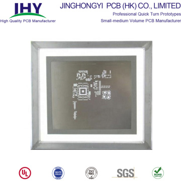
PCB Assembly SMT PCB Stencil PCB Stencil Maker
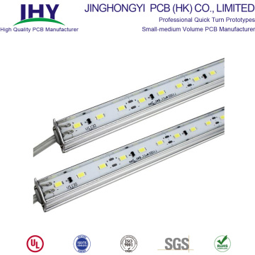
High Quality 24V LED PCB Circuit Board Assembly
Customized Single-sided 12V SMD LED PCB Circuit Board
Related ProductsProduct Categories-
PCB Prototype(97)
-
Quick Turn PCB(33)
-
LED PCB(114)
-
Single Sided PCB(15)
-
Double Sided PCB(60)
-
Multilayer PCB(149)
-
Rigid PCB(22)
-
Flexible PCB(48)
-
Rigid Flex PCB(43)
-
Aluminum PCB(62)
-
Metal Core PCB(50)
-
Thick Copper PCB(106)
-
HDI PCB(61)
-
Impedance Control PCB(27)
-
BGA PCB(11)
-
High TG PCB(32)
-
Fr4 PCB(44)
-
Gold Fingers PCB(29)
-
PCB Application(5)
-
PCB Stencil(56)
-
PCB Assembly Service(67)
-
High Frequency PCB(47)


