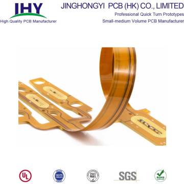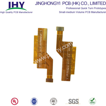

2 Layer Flexible PCB
- Payment Type:
- L/C, T/T, D/P, Paypal, Money Gram, Western Union
- Incoterm:
- FOB, CFR, CIF, EXW, FCA, CPT, CIP
- Min. Order:
- 1 Piece/Pieces
- Min. Order:
- 1 Piece/Pieces
- Transportation:
- Ocean, Air
Your message must be between 20 to 2000 characters
Contact Now| Place of Origin: | China |
|---|---|
| Productivity: | 10000 |
| Payment Type: | L/C,T/T,D/P,Paypal,Money Gram,Western Union |
| Incoterm: | FOB,CFR,CIF,EXW,FCA,CPT,CIP |
| Certificate: | ISO9001 |
| Transportation: | Ocean,Air |
2 Layer/Double layer Flexible PCB
Flexible circuit boards, Flexible PCB are certainly useful, but they are not going to replace rigid circuit boards for all applications. Cost efficiency is the main obstacle to implementing an exclusively flexible circuit board design in a consumer product. Rigid circuit boards are less expensive to manufacture and install in a typical automated high-volume fabricating facility.
Double layer flexible circuit board signifies that there are two layers of copper circuitry. In most cases, the two layers of copper are electrically connected by drilling small holes through the copper circuits and the separating dielectric, then plating the holes with copper to make a connection between them.
Typically, the ideal solution for an innovative product is one that incorporates flexible circuitry when necessary, and employs solid, reliable rigid circuit boards where possible to keep manufacturing and assembly costs down.
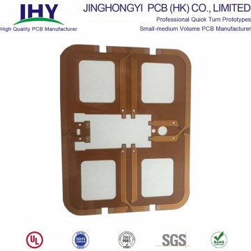
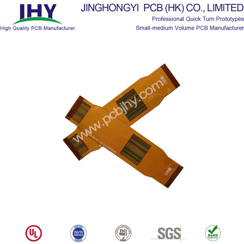
Construction for Double Layer Flexible Circuit Board


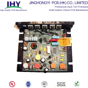
The application for this double layer flex circuit is a keypad used on a hand held device. There are components assembled on the flex: a ZIF (zero insertion force) connector interface and LEDs (light emitting diodes).

Top Stiffener - Stiffeners are created to give flex circuits rigid areas where required. Stiffeners in most instances are made of printed circuit board, but can also be metal, ceramic and even additional layers of polyimide.

Top Silkscreen - The images will be printed onto the top of the finished circuit with indelible ink. This assists with component placement.

Top Coverlay - This is the top polyimide cover that adheres to the first layer of etched copper.

Layer 1 - This is the first layer of copper that PFC will etch.

Layer 2 - This is the second layer of copper to be etched. There will be a layer of dielectric material between the layers of copper.

Bottom Coverlay - The bottom coverlay is the polyimide dielectric material that covers the second layer of copper. The circuit is now encapsulated on top and bottom with polyimide.

Drill File - The drill file designates the location of the holes to be drilled in the circuit. The circuit layers (copper and coverlays) will be pressed together, drilled, then run through plating to put copper in the holes and make connections from the top copper layer to the bottom.

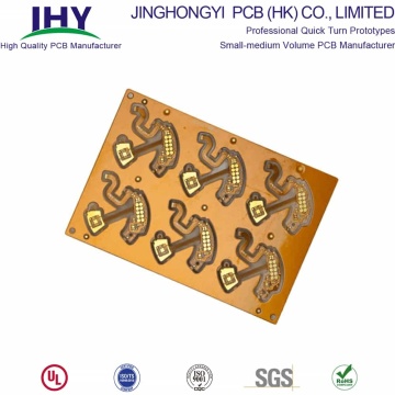
Outline - PFC`s flex are manufactured in 18"x12" or 18"x24" panels. We fit as many parts as possible on a panel then use a punch/die to cut the parts from the panel. This is the artwork for the tooling die to cut the part from the panel.

Completed Circuit - There are additional steps to making a circuit, such as plating, etching, pressing, electrical test, inspection and assembling that are not shown in the artwork slides.
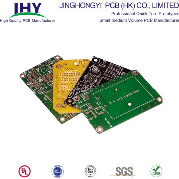
China Flexible PCB Manufacturer
Find a Flexible PCB Manufacturer and Supplier. Choose Quality Flexible PCB Manufacturers, Suppliers, Exporters at PCBJHY.com
JHY PCB specialized manufacturers from China, Flex PCB, Flexible Printed Circuit suppliers/factory, wholesale high-quality products of Flexi Circuits and manufacturing, we have the perfect after-sales service and technical support. Look forward to your cooperation!
In addition to providing high-quality products, we sincerely reduce the cost of products and provide cheaper prices for our customers in order to make them feel very satisfied.
Products & Services
- Quick Turn PCB
- Rigid PCB
- Flexible PCB
- Rigid-flex PCB
- Aluminum PCB
- PCB Stencil
- Multilayer PCB
What is Flexible PCB?
Flexible circuits (also variously referred to around the globe as flex circuits, flexible printed circuit boards, flex print, flexi-circuits) are members of electronic and interconnection family. They consist of a thin insulating polymer film having conductive circuit patterns affixed thereto and typically supplied with a thin polymer coating to protect the conductor circuits.
The technology has been used for interconnecting electronic devices since the 1950s in one form or another. It is now one of the most important interconnection technologies in use for the manufacture of many of today's most advanced electronic products.
In practice there are many different kinds of flexible circuits, including one metal layer, double sided, multilayer and rigid flex circuits. The circuits can be formed by etching metal foil cladding (normally of copper) from polymer bases, plating metal or printing of conductive inks among other processes.
Flexible circuits may or may not have components attached. When components are attached, they are considered by some in the industry to be flexible electronic assemblies.
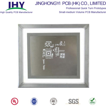
2 Layer Flexible PCB Fabrication


Flexible PCB Manufacturing Capability
Learn more about JHY PCB by exploring the manufacturing capability of Flexible PCB below. We can do more than you can imagine.
| Items | Manufacturing Capability | |
| PCB Layers | 1 - 8layers | |
| Laminate | DuPont PI, Shengyi PI | |
| Maximum PCB Size(Length x Width) | Single Sided PCB | 480*4000mm |
| Double Sided PCB | 480*1800mm | |
| Multilayers | 236*600mm | |
| Minimum Board Thickness | Single Sided PCB | 0.05mm+/-0.02mm |
| Double Sided PCB | 0.08mm+/-0.02mm | |
| Multilayers | As per Gerber | |
| Finished Board Thickness | 1-6L | 0.05mm-0.6mm |
| 8L | 1.6mm | |
| Min Tracing/Spacing | Copper Thickness 1/3 oz: | 0.076mm/0.076mm (1-6L) |
| 0.05mm/0.05mm (8L) | ||
| Copper Thickness 1/2 oz: | 0.076mm/0.076mm (1-6L) | |
| 0.06mm/0.06mm (8L) | ||
| Copper Thickness 1oz: | 0.1mm/0.1mm (1-6L) | |
| 0.065mm/0.065mm (8L) | ||
| Min. Annular Ring | 4mil | |
| Minimum Hole Size | 1-6L | 0.2mm(8mil) (CNC) |
| 8L | 0.15mm(CNC) | |
| Solder Mask Color | Green, White, Blue, Black, Red, Yellow | |
| Solder-stop coating---Coverlay | PI and PET film |
|
| Silkscreen Color | White, Black, Yellow |
|
| Surface Finish | OSP | |
| e HASL | ||
| ENIG(Electroless NickLead-Freeion Gold) | Ni thickness:2-6um | |
| Au thickness:0.025-0.05um | ||
| Flash Gold | Ni thickness:2-8um | |
| Au thickness:0.025-0.15um | ||
| Immersion Tin | Tin thickness:0.5-1um | |
| PlatingTin | Tin thickness:1-10um | |
| Laser cuPunching | ||
| Special technologies | Peelable solder mask | |
| Gold fingers | ||
| Stiffener (only for PI/FR4 substrate) | ||
| Impedance Control+/-10% | ||
| Rigid Flex PCB | ||
Related Keywords
-
PCB Assembly SMT PCB Stencil PCB Stencil Maker
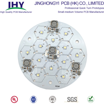
High Quality 24V LED PCB Circuit Board Assembly
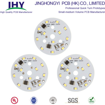
Customized Single-sided 12V SMD LED PCB Circuit Board
Related ProductsProduct Categories-
PCB Prototype(97)
-
Quick Turn PCB(33)
-
LED PCB(114)
-
Single Sided PCB(15)
-
Double Sided PCB(60)
-
Multilayer PCB(149)
-
Rigid PCB(22)
-
Flexible PCB(48)
-
Rigid Flex PCB(43)
-
Aluminum PCB(62)
-
Metal Core PCB(50)
-
Thick Copper PCB(106)
-
HDI PCB(61)
-
Impedance Control PCB(27)
-
BGA PCB(11)
-
High TG PCB(32)
-
Fr4 PCB(44)
-
Gold Fingers PCB(29)
-
PCB Application(5)
-
PCB Stencil(56)
-
PCB Assembly Service(67)
-
High Frequency PCB(47)