

hybrid Dielectric PCB Prototype Fabrication
Quantity:
Your message must be between 20 to 2000 characters
Contact NowBasic Info
Basic Info
Product Description
Product Description
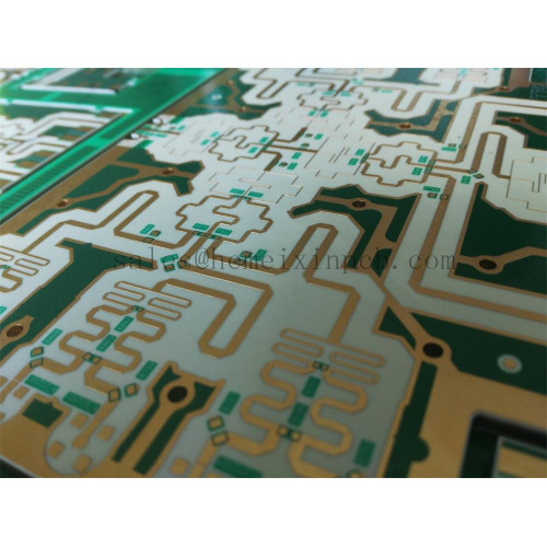
The hybrid Dielectric PCB stack-up can be used as one of enablers to improve SI for signals routed on selected layers. For a hybrid PCB stack-up, some layers of the PCB use low loss dielectric while the others are fabricated with the traditional FR4. The cost of such a hybrid stack-up is normally lower than all low loss material PCB stack-up, but with the advantage of some routing layers having the same or similar low loss properties as an all low loss stack-up, thus achieving optimized cost-performance.


Related Keywords
Related Keywords
You May Also Like
You May Also Like
-
Prototype Polyimide Flexible pcb
Prototype Kapton PCB assembly

Microelectronic Assembly Prototyping
Related ProductsProduct Categories-
Microvia PCB(1)
-
Microwave PCB(13)
-
Heavy Copper PCB(4)
-
Metal Core PCB(10)
-
Turn-key PCB Assembly(19)
- Circuit Board Assembly(1)
- PCB Assembly(1)
- Rigid PCB Assembly(1)
- PCB Board Assembly(1)
- Circuit Card Assembly(1)
- SMT PCB(1)
- PCB Turnkey(1)
- Pcb Assembly Manufacturer(1)
- Pcb Assembly Quote(1)
- Pcb Assy(1)
- Electro Mechanical Assembly(1)
- Electronic Circuit Board Assembly(1)
- Pcb Manufacturing And Assembly(1)
- Electronic PCB Contract Manufacturing(1)
- Electronic PCB Assembly(1)
- Microelectronic Assembly(1)
- RF PCB Assembly(1)
- Wireless PCB Assembly(1)
- Turnkey PCB Assembly(1)
-
Rigid Flex PCB Assembly(12)
- Rigid Flexible Circuits Assembly(1)
- Rigid-flex Circuits Assembly(1)
- Flex-rigid Circuits Assembly(1)
- Flex-rigid Pcb Assembly(1)
- Rigid Flexible PCB Assembly(1)
- Rigid Flex Circuit Assembly(1)
- Rigid Flex Circuits Assembly(1)
- Flex Rigid PCB Assembly(1)
- Semiflex Pcb Assembly(1)
- Starr Flex PCB Assembly(1)
- Rigiflex Pcb Assembly(1)
- Rigid-Flexible PCB Assembly(1)
-
PCB Prototype Assembly(2)
-
Flexible Circuits Assembly(15)
- Flex Printed Circuits Assembly(1)
- Multilayer Flexible PCB Assembly(1)
- Microvia Flex Circuit Assembly(1)
- Flat Flex PCB Assembly(1)
- Flex Cable Circuit Board Assembly(1)
- Flexible Circuitry Assembly(1)
- HDI Flexible PCB Assembly(1)
- Microvia Flex PCB Assembly(1)
- HDI Flexible Circuit Assembly(1)
- Kapton PCB Assembly(1)
- Polyimide Pcb Assembly(1)
- Kapton Flexible PCB Assembly(1)
- Polyimide Flexible Circuit Assembly(1)
- Flex PCB Assembly(1)
- Flexible Printed Circuit Board Assembly(1)
-
PCB Assembly(9)
-
Flexible Circuits(19)
- Flex Printed Circuits(1)
- Multilayer Flexible PCB(1)
- Flexible Heater(1)
- Flat Flex PCB(1)
- Flex Cable Circuit(1)
- Flexible Circuitry(1)
- HDI Multilayer Flexible PCB(1)
- Microvia Flex PCB(1)
- HDI Flexible Circuit(1)
- Microvia Flex Circuit(1)
- Flex Pcb Manufacturer(1)
- Flex Pcb Fabrication(1)
- Flexible Circuit Board(1)
- Flex PCB(1)
- Kapton PCB(1)
- Polyimide Pcb(1)
- Kapton Flexible PCB(1)
- Polyimide Flexible Circuit(1)
- Flexi Circuits(1)
-
Rigid Flex PCB(11)

