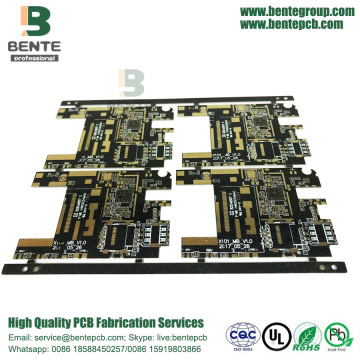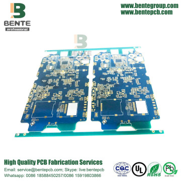

FR4 Tg170 HDI PCB ENIG
- Payment Type:
- L/C, T/T, D/P, Paypal, Money Gram, Western Union
- Incoterm:
- FOB, CFR, CIF, FCA, CPT, CIP
- Min. Order:
- 1 Piece/Pieces
- Min. Order:
- 1 Piece/Pieces
- Delivery Time:
- 5 Days
- Transportation:
- Ocean, Land, Air
Your message must be between 20 to 2000 characters
Contact Now| Place of Origin: | China |
|---|---|
| Productivity: | 10000 |
| Payment Type: | L/C,T/T,D/P,Paypal,Money Gram,Western Union |
| Incoterm: | FOB,CFR,CIF,FCA,CPT,CIP |
| Certificate: | ISO 9001 |
| Transportation: | Ocean,Land,Air |
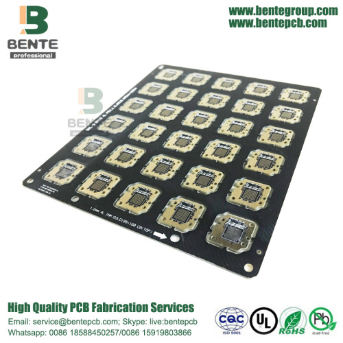
Product Description:
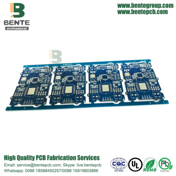
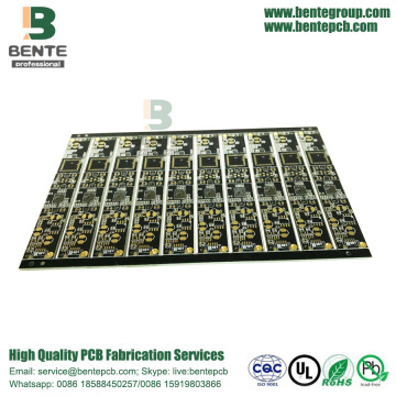
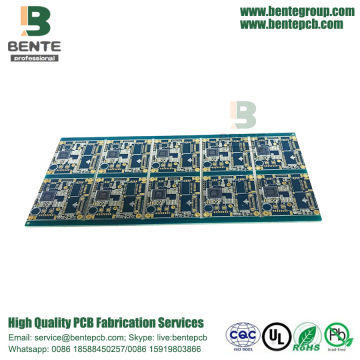
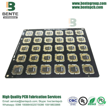
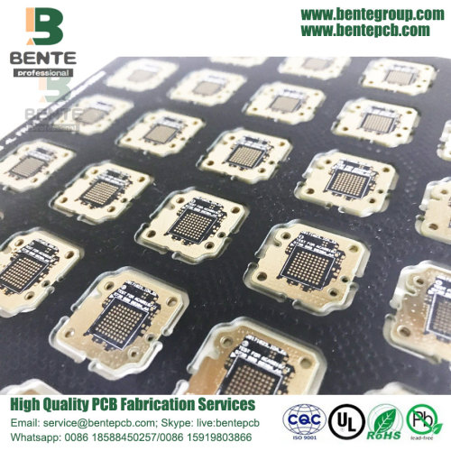
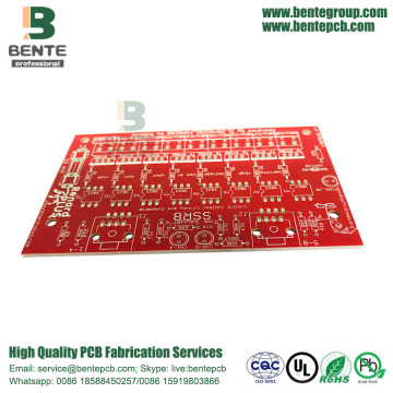
4 Layers HDI PCB, Material is FR4, Tg170, Thickness is 1.6mm, Finished Copper is 1oz, Surface Treatment is ENIG, The Field of Application is Micro-electronic Communications Equipment, Process Characteristics are Buried Blind Hole, High TG, PCB Manufacturing Process, Circuit Board Printer, PCB Board Design.
BentePCB, the current plant actually occupies an area of 6,000 square meters, process capacity of 8,000 square meters / month, mainly to Allegro, mainly small and medium-sized orders.
Good News: Every orders will get free SMT stencil , please check out our website at www.bentepcb.com/onlinepcb.htm
HDI PCB:
High Density Interconnects (HDI) are used to meet the market demand for complex designs in smaller form factors across the majority of market segments, (Wireless, Telecom, Military, Medical, Semiconductor, and Instrumentation).
HDI Circuit boards, one of the fastest growing technologies in PCBs, HDI Boards contain blind and/or buried vias and often contain microvias of .006 or less in diameter.
They have finer lines and spaces always = <3mil They have a higher circuitry density than traditional circuit boards.
Andwin maintains years of experience with HDI products and was a pioneer of second generation microvias. now offer an entire family of microvia technology solutions for your next generation products.
Stack up of HDI PCB
Stack up of 1 Step HDI PCB

Stack up of 2 step HDI PCB

Stack up of 2 steps HDI with blind via and buried via

Anylayer connect of HDI PCB, need to adjust drill

About Us:
BentePCB is a professional PCB manufacturing which is focus on double side, multilayer, HDI PCB, rigid PCB and flexible PCB mass production. The company was established on 2011.
We have two factories together, The factory in Shenzhen is specialized in small and middle volume orders and the factory in Jiangxi is for big volume.
Why Us?
UL (E492586), ISO9001, ISO14001, TS16949, RoHS certified.
Turnover USD 10-50 million per year.
15,000 sqm area, 450 staff .
Mass Production from single to 16 layers.
Special Material:ROGERS, Arlon, Taconic.etc.
Client:Huawei, SAMSUNG, Malata, Midea,Texas Instruments.etc.
Certification(UL:E492586, TS16949, ISO14001, ISO9001,RoHS):


Factory Tour:


Exhibition:
We Took part in the famous exhibitions over the past years,and got highly appreciation from the top experts,as well as cooperated tightly with them.

Delivery:
BentePCB offers flexible shipping methods for our customers, you may choose from one of the methods below.


We don`t just sell PCBs .We sell sleep.

Related Keywords
-
LED PCB LED Lighting
LED PCB Aluminum PCB
PCB Prototype Red ink
Related ProductsProduct Categories-
Standard PCB(60)
-
Aluminum PCB(6)
-
Multilayer PCB(66)
-
Prototype PCB(50)
-
Quickturn PCB(31)
-
Metal PCB(5)
-
Low Cost PCB(30)
-
HDI PCB(22)
-
Flexible PCB(18)
-
Flex Rigid PCB(9)
-
Thick Copper PCB(27)
-
High-Tg PCB(25)
-
High Precision Multilayer PCB(75)
-
Custom PCB(31)
-
SMD Stencil(4)
-
Heavy Copper PCB(13)
-
PCB Prototype(32)
-
LED PCB(3)