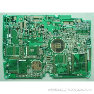
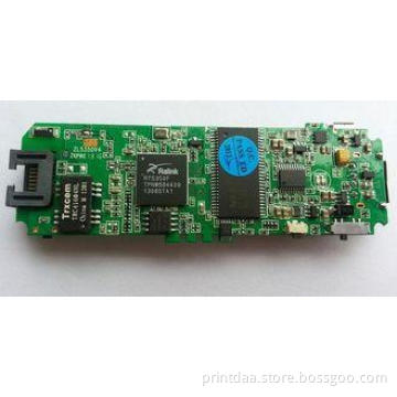
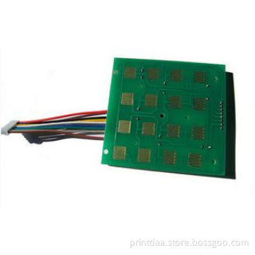
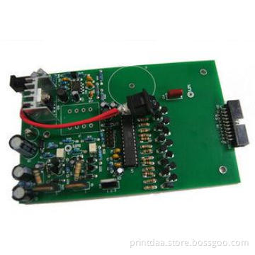
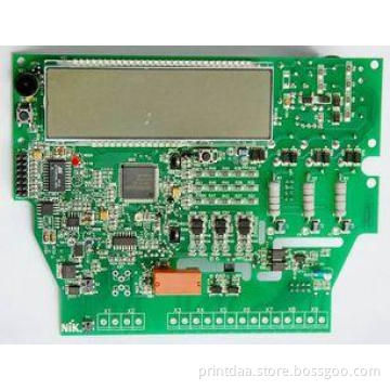
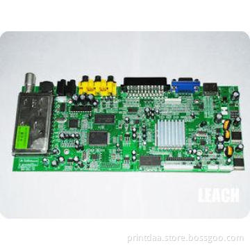
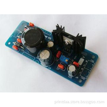
Green Power Supply PCB 2 Layer Double Sided Printed Circuit
- Min. Order:
- 1
- Min. Order:
- 1
- Delivery Time:
- 30 Days
Your message must be between 20 to 2000 characters
Contact Now| Place of Origin: | China |
|---|
Green Power Supply PCB 2 Layer Double Sided Printed Circuit Board Assembly
Specification
- Layer: 2 Layer
- Material: FR4
- Board Thickness: 1.0mm
- Surface Treatment: Lead-Free HASL
- Solder Mask: Green
- Size: 288.77 x 197.26mm
- Copper Thickness: 1.0oZ
- Min. Line Spacing: 0.75mm
- Min Trace Space: 1.5mm
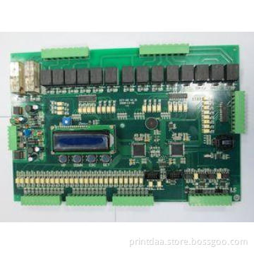
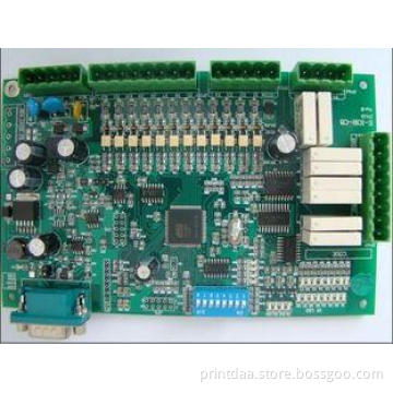
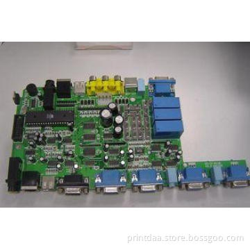
Huaswin specialized in PCB manufacturing and and PCB Assembly
PCBA capabilities:
Fast prototyping
High mix, low and medium volume build
SMT MinChip:0201
BGA: 1.0 to 3.0 mm pitch
Through-hole assembly
Special processes (such as conformal coating and potting)
ROHS capability
IPC-A-610E and IPC/EIA-STD workmanship operation
Detailed Specification of PCB Manufacturing
|
1 |
layer |
1-30 layer |
|
2 |
Material |
CEM-1, CEM-3 FR-4, FR-4 High TG, |
|
3 |
Board thickness |
0.2mm-6mm |
|
4 |
Max.finished board size |
800*508mm |
|
5 |
Min.drilled hole size |
0.25mm |
|
6 |
min.line width |
0.075mm(3mil) |
|
7 |
min.line spacing |
0.075mm(3mil) |
|
8 |
Surface finish |
HAL, HAL Lead free,Immersion Gold/ |
|
9 |
Copper thickness |
0.5-4.0oz |
|
10 |
Solder mask color |
green/black/white/red/blue/yellow |
|
11 |
Inner packing |
Vacuum packing,Plastic bag |
|
12 |
Outer packing |
standard carton packing |
|
13 |
Hole tolerance |
PTH:±0.076,NTPH:±0.05 |
|
14 |
Certificate |
UL,ISO9001,ISO14001,ROHS,TS16949 |
|
15 |
Profiling punching |
Routing,V-CUT,Beveling |
PCB Assembly services:
SMT Assembly
Automatic Pick & Place
Component Placement as Small as 0201
Fine Pitch QEP - BGA
Automatic Optical Inspection
Through-hole Assembly
Wave Soldering
Hand Assembly and Soldering
Material Sourcing
IC pre-programming / Burning on-line
Function testing as requested
Aging test for LED and Power boards
Complete unit assembly (which including plastics, metal box, Coil, cable assembly etc)
Packing design
Conformal coating
Both dip-coating and vertical spray coating is available. Protecting non-conductive dielectric layer that is
applied onto the printed circuit board assembly to protect the electronic assembly from damage due to
contamination, salt spray, moisture, fungus, dust and corrosion caused by harsh or extreme environments.
When coated, it is clearly visible as a clear and shiny material.
Complete box build
Complete 'Box Build' solutions including materials management of all components, electromechanical parts,
plastics, casings and print & packaging material
Testing Methods
AOI Testing
Checks for solder paste
Checks for components down to 0201"
Checks for missing components, offset, incorrect parts, polarity
X-Ray Inspection
X-Ray provides high-resolution inspection of:
BGAs
Bare boards
In-Circuit Testing
In-Circuit Testing is commonly used in conjunction with AOI minimizing functional defects caused by
component problems.
Power-up Test
Advanced Function Test
Flash Device Programming
Functional testing
Quality Processes:
1. IQC: Incoming Quality Control (Incoming Materials Inspection)
2. First Article Inspection (FAI) for every process
3. IPQC: In Process Quality Control
4. QC: 100% Test & Inspection
5. QA: Quality Assurance based on QC inspection again
6. Workmanship: IPC-A-610, ESD
7. Quality Management based on CQC, ISO9001:2008, ISO/TS16949