One Stop PCB Fabrication to PCB Assembly
- Payment Type:
- T/T, Paypal, Western Union
Quantity:
Your message must be between 20 to 2000 characters
Contact NowBasic Info
Basic Info
| Place of Origin: | Shenzhen, China |
|---|---|
| Payment Type: | T/T, Paypal, Western Union |
Product Description
Product Description
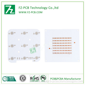
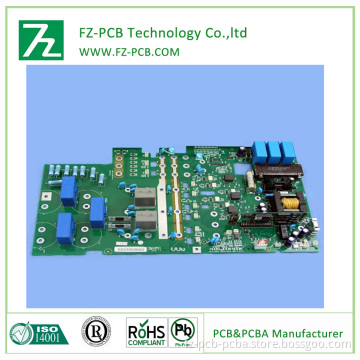
High technology 1~16layers PCB's, 1~8 layers PCBA assebly, 0.2~3.2mm thickness, 0.3~4.0oz copper thickness
FR4, FR4(TG130,150,170), FR1,CEM-1, CEM3, Aluminum based, HF (Rogers,Teflon)
HDI and Sequential Lamination
Flexible, Flex-rigid and Rigid PCBs
RoHS/UL, ISO9001:2008 & ISO/TS16949:2009, ISO14001:2004
What will you get from FZ-PCB
Reliable and stable quality with more than 12 years pcb manufacturing experience.
Quick response & 24 hours available service.
Professional sales service & advice.
Fulfillment of our promises, NO lies.
Protecting your Intellectual property. All our staff of trained professionals are working under a strict confidential contract.
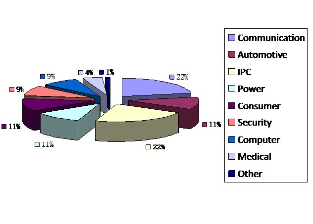
Market Segment
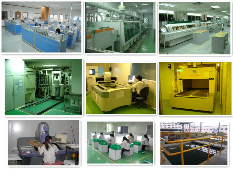
 Factory glance
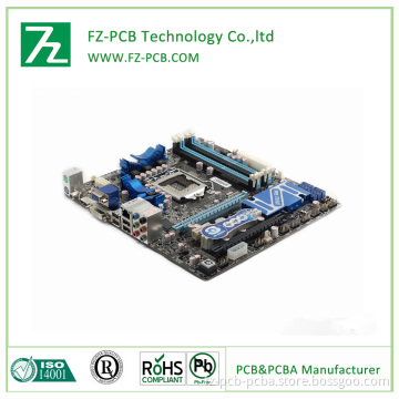
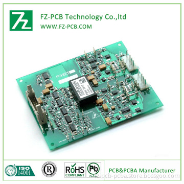
 PCBA Capabilities included
·Components procerement, PCB and accessories manufacturing, PCB Assembly, mechanical and final assembly, Electronic testing and function testing.
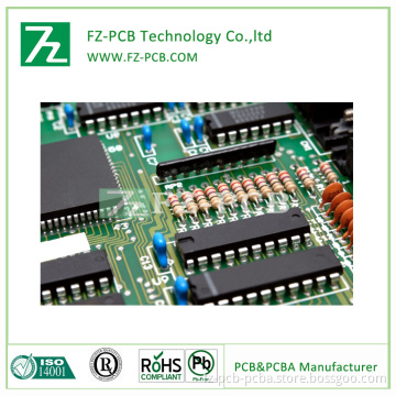
·High precision0402, 0603, 0805, 1210 and 2512; fine pitch QFP(0.3mm), BGA(0.5mm), IC(0.3mm) bonding size components SMT technology and lead free RoHS technology.
·Circuit boards with 1 to 8 layers PCB layout, modification, fabrication, plastics, metal box building, final assembly and testing.
·ISO 9001-2000 certification and elevator safety report.
PCBA building experience range
·Industrial elevator system, digital video record (DVR) system, medical, computing, storage, instrumentation, traffic, industrial power, fire alarm, wireless communication, telecommunication, networking and house controller.
Package & Shipping Method:
1. Vacuum package with silica gel, Carton box with packing belt.
2. By DHL, UPS, FedEx, TNT
3. By EMS (Usually for Russia Clients)
4. By sea for mass quantity according to customer's requirement
Payment method
1. T/T
2. Paypal
3. Western Union
FR4, FR4(TG130,150,170), FR1,CEM-1, CEM3, Aluminum based, HF (Rogers,Teflon)
HDI and Sequential Lamination
Flexible, Flex-rigid and Rigid PCBs
RoHS/UL, ISO9001:2008 & ISO/TS16949:2009, ISO14001:2004
What will you get from FZ-PCB
Reliable and stable quality with more than 12 years pcb manufacturing experience.
Quick response & 24 hours available service.
Professional sales service & advice.
Fulfillment of our promises, NO lies.
Protecting your Intellectual property. All our staff of trained professionals are working under a strict confidential contract.
Market Segment
Factory glance PCBA Capabilities included·Components procerement, PCB and accessories manufacturing, PCB Assembly, mechanical and final assembly, Electronic testing and function testing.
·High precision0402, 0603, 0805, 1210 and 2512; fine pitch QFP(0.3mm), BGA(0.5mm), IC(0.3mm) bonding size components SMT technology and lead free RoHS technology.
·Circuit boards with 1 to 8 layers PCB layout, modification, fabrication, plastics, metal box building, final assembly and testing.
·ISO 9001-2000 certification and elevator safety report.
PCBA building experience range
·Industrial elevator system, digital video record (DVR) system, medical, computing, storage, instrumentation, traffic, industrial power, fire alarm, wireless communication, telecommunication, networking and house controller.
Package & Shipping Method:
1. Vacuum package with silica gel, Carton box with packing belt.
2. By DHL, UPS, FedEx, TNT
3. By EMS (Usually for Russia Clients)
4. By sea for mass quantity according to customer's requirement
Payment method
1. T/T
2. Paypal
3. Western Union
| Files | Gerber, Protel, Powerpcb, Autocad, Orcad, etc |
| Material | FR-4, Hi-Tg FR-4, Lead free Materials (RoHS Compliant) , FR1, CEM-3, CEM-1, Aluminium, High frequency Material (Rogers, Teflon, Taconic), Polymide. |
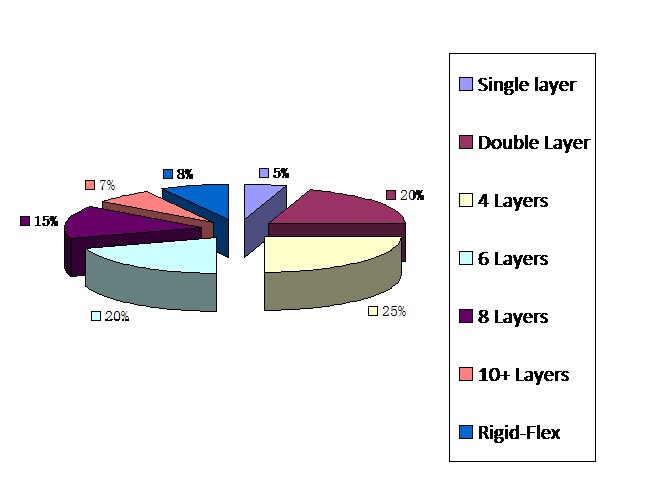
| Layer No. | 1 - 16 Layers |
| Board thickness | 0.0075"(0.2mm)-0.125"(3.2mm) |
| Board Thickness Tolerance | ±10% |
| Copper thickness | 0.3OZ - 4OZ |
| Impedance Control | ±10% |
| Warp and Twist | ≤0.075% |
| Peel Strength | ≥61B/in(≥107g/mm) |
| Min Trace Width (a) | 3mil |
| Min Space Width (b) | 3mil |
| Min Annular Ring | 0.004"(0.1mm) |
| SMD Pitch (a) | 0.012"(0.3mm) |
| pcb with green solder mask and LF-FREE surface finishing BGA Pitch (b) | 0.027"(0.675mm) |
| Register tolerance | 0.05mm |
| Min Solder Mask Dam (a) | 0.005"(0.125mm) |
| Solder mask Clearance (b) | 0.005"(0.125mm) |
| Min SMT Pad spacing (c) | 0.004"(0.1mm) |
| Solder Mask Thickness | 0.0007"(0.018mm) |
| Hole size | 0.008"(0.20mm)-- 0.257"(6.5mm) |
| Hole Size Tol (+/-) | ±0.003"(±0.0762mm) |
| Max PTH Aspect Ratio | 10:1 |
| Hole Registration | 0.003"(0.075mm) |
| HASL | 2.5um |
| Lead free HASL | 2.5um |
| Immersion Gold | Nickel 3-7um Au:1-3u'' |
| OSP | 0.2-0.5um |
| Panel Outline Tol (+/-) | ±0.004''(±0.1mm) |
| Beveling | 30°45° |
| V-cut | 15° 30° 45° 60° |
| Surface finish | HAL, HASL Lead Free, Immersion gold, Gold plating, Gold finger, immersion silver, immersion Tin, OSP, Carbon ink, |
| Certificate | ROHS ISO9001 TS16949 SGS UL |
| Special requirements | Buried&blind vias, Impedance control, via plug, BGA soldering and gold finger |
Related Keywords
Related Keywords
You May Also Like
You May Also Like