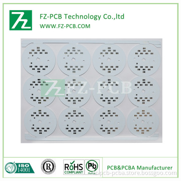
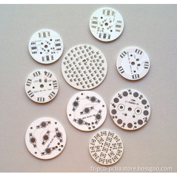
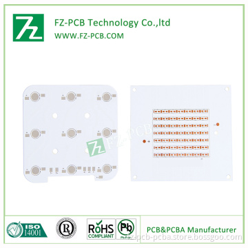
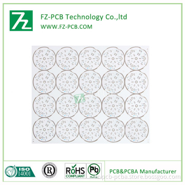
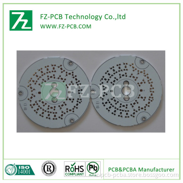
Cem-1 Circuit Board LED PCB
- Payment Type:
- T/T, Paypal, Western Union
Quantity:
Your message must be between 20 to 2000 characters
Contact NowBasic Info
Basic Info
| Place of Origin: | Shenzhen, China |
|---|---|
| Payment Type: | T/T, Paypal, Western Union |
Product Description
Product Description
Specialize in CEM-1 LED PCB with competitive price in LED PCB line
High technology 1~16layers PCBs from 0.2~3.2mm thickness with 0.3~6.0oz copper thickness
FR4, FR4(TG130,150,170), FR1,CEM-1, CEM3, Aluminum based, HF (Rogers,Teflon)
RoHS/UL, ISO9001:2008 & ISO14001/TS16949:2009
Package & Shipping Method:
1. Vacuum package with silica gel, Carton box with packing belt.
2. By DHL, UPS, FedEx, TNT
3. By EMS (Usually for Russia Clients)
4. By sea for mass quantity according to customer's requirement
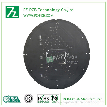
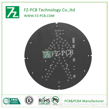
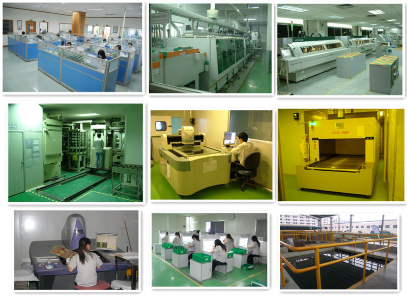
Factory glance
High technology 1~16layers PCBs from 0.2~3.2mm thickness with 0.3~6.0oz copper thickness
FR4, FR4(TG130,150,170), FR1,CEM-1, CEM3, Aluminum based, HF (Rogers,Teflon)
RoHS/UL, ISO9001:2008 & ISO14001/TS16949:2009
Package & Shipping Method:
1. Vacuum package with silica gel, Carton box with packing belt.
2. By DHL, UPS, FedEx, TNT
3. By EMS (Usually for Russia Clients)
4. By sea for mass quantity according to customer's requirement
Factory glance
| Files | Gerber, Protel, Powerpcb, Autocad, Orcad, etc |
| Material | FR-4, Hi-Tg FR-4, Lead free Materials (RoHS Compliant) , FR1, CEM-3, CEM-1, Aluminium, High frequency Material (Rogers, Teflon, Taconic), Polymide. |
| Layer No. | 1 - 16 Layers |
| Board thickness | 0.0075"(0.2mm)-0.125"(3.2mm) |
| Board Thickness Tolerance | ±10% |
| Copper thickness | 0.3OZ - 4OZ |
| Impedance Control | ±10% |
| Warp and Twist | ≤0.075% |
| Peel Strength | ≥61B/in(≥107g/mm) |
| Min Trace Width (a) | 3mil |
| Min Space Width (b) | 3mil |
| Min Annular Ring | 0.004"(0.1mm) |
| SMD Pitch (a) | 0.012"(0.3mm) |
| pcb with green solder mask and LF-FREE surface finishing BGA Pitch (b) | 0.027"(0.675mm) |
| Register tolerance | 0.05mm |
| Min Solder Mask Dam (a) | 0.005"(0.125mm) |
| Solder mask Clearance (b) | 0.005"(0.125mm) |
| Min SMT Pad spacing (c) | 0.004"(0.1mm) |
| Solder Mask Thickness | 0.0007"(0.018mm) |
| Hole size | 0.008"(0.20mm)-- 0.257"(6.5mm) |
| Hole Size Tol (+/-) | ±0.003"(±0.0762mm) |
| Max PTH Aspect Ratio | 10:1 |
| Hole Registration | 0.003"(0.075mm) |
| HASL | 2.5um |
| Lead free HASL | 2.5um |
| Immersion Gold | Nickel 3-7um Au:1-3u'' |
| OSP | 0.2-0.5um |
| Panel Outline Tol (+/-) | ±0.004''(±0.1mm) |
| Beveling | 30°45° |
| V-cut | 15° 30° 45° 60° |
| Surface finish | HAL, HASL Lead Free, Immersion gold, Gold plating, Gold finger, immersion silver, immersion Tin, OSP, Carbon ink, |
| Certificate | ROHS ISO9001 TS16949 SGS UL |
| Special requirements | Buried&blind vias, Impedance control, via plug, BGA soldering and gold finger |

Related Keywords
Related Keywords