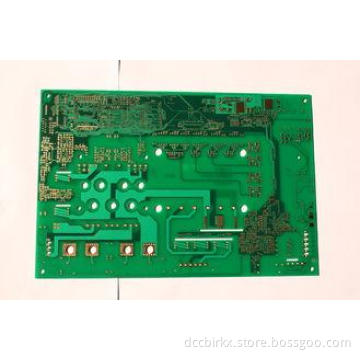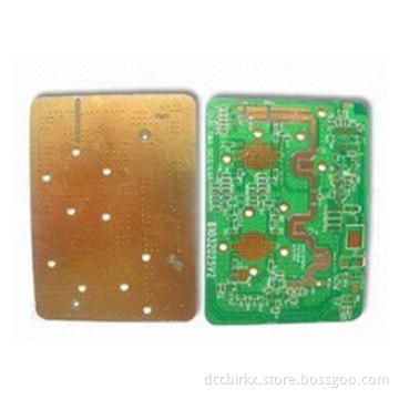
Double Layer Heavy Copper PCB 4 oz Copper Green Solder Mask
- Min. Order:
- 1
- Min. Order:
- 1
- Delivery Time:
- 30 Days
Your message must be between 20 to 2000 characters
Contact Now| Place of Origin: | China |
|---|
PCB Capability
|
|
High precision prototype |
PCB bulk production |
|
|
Max Layers |
1-28 layers |
1-14 layers |
|
|
MIN Line width(mil) |
3mil |
4mil |
|
|
MIN Line space(mil) |
3mil |
4mil |
|
|
Min via (mechanical drilling) |
Board thickness≤1.2mm |
0.15mm |
0.2mm |
|
Board thickness≤2.5mm |
0.2mm |
0.3mm |
|
|
Board thickness>2.5mm |
Aspect Ration≤13:1 |
Aspect Ration≤13:1 |
|
|
Aspect Ration |
Aspect Ration≤13:1 |
Aspect Ration≤13:1 |
|
|
Board thickness |
MAX |
8mm |
7mm |
|
MIN |
2 layers:0.2mm;4 layers:0.35mm;6 layers:0.55mm;8 layers:0.7mm;10 layers:0.9mm |
2 layers:0.2mm;4 layers:0.4mm;6 layers:0.6mm;8layers:0.8mm |
|
|
MAX Board size |
610*1200mm |
610*1200mm |
|
|
Max copper thickness |
0.5-6oz |
0.5-6oz |
|
|
Immersion Gold/ Gold Plated Thickness |
Immersion Gold:Au,1—8u” |
|
|
|
Hole copper thick |
25um 1mil |
25um 1mil |
|
|
Tolerance |
Board thickness |
Board thickness≤1.0mm:+/-0.1mm |
Board thickness≤1.0mm:+/-0.1mm |
|
Outline Tolerance |
≤100mm:+/-0.1mm |
≤100mm:+/-0.13mm |
|
|
Impedance |
±10% |
±10% |
|
|
MIN Solder mask bridge |
0.08mm |
0.10mm |
|
|
Plugging Vias capability |
0.25mm--0.60mm |
0.70mm--1.00mm |
|
Design Guide for Heavy Copper PCB
Typical conductor width/spacing/thickness tolerance is +/-20%, although tighter tolerance is achievable.
The minimum width and thickness of a heavy copper PCB conductor is determined primarily on the basis of the current carrying capacity required and the maximum permissible conductor temperature rise.
A circuit board trace, depending on its size and manufacturing process, may not be rectangular in shape. Heavy copper conductors can significantly add to the overall board thickness.
Additive (plating) processed are preferred to subtractive (etching) processes but are more expensive).
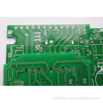
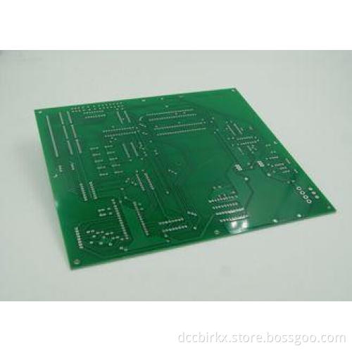
Heavy Copper PCB General Info
Heavy Copper Board does not have a set of definition per IPC. According to PCB industry, however, peopel generally use this name to identify a printed circuit board with copper conductors 3 oz/ft2 - 10 oz/ft2 in inner and/or outer layers. And Extreme heavy copper PCB refers to 20 oz/ft2 to 200 oz/ft2 printed circuit board
Heavy copper normally used for a various products but not limited to: high power distribution, heat dissipation, planar transformers, power convertors, and so on
Capability of Heavy Copper PCB
Base material: FR4/Aluminum
Copper thickness: 4 OZ~10 OZ
Extreme Heavy Copper: 20~200 OZ
Outline: Routing, punching, V-Cut
Soldermask: White/Black/Blue/Green/Red Oil
Surface finishing: Immersion Gold, HASL, OSP