High efficiency step-up dc-dc converters 100W Output 5Volt
- Min. Order:
- 1
- Min. Order:
- 1
- Delivery Time:
- 30 Days
Your message must be between 20 to 2000 characters
Contact Now| Place of Origin: | China |
|---|
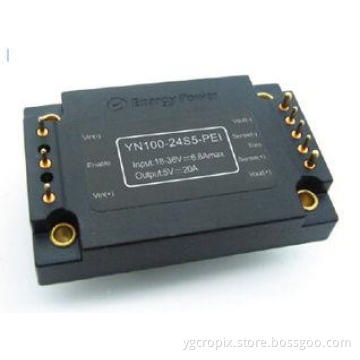
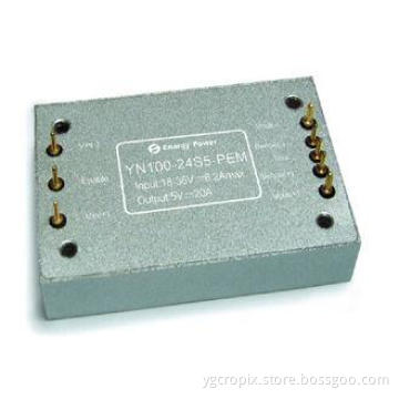
DC-DC Converters 100W Output 5V YN100-24S5-PEI
Key Features
Output power: 100W
Wide input range: 18-36Vdc
High conversion efficiency: Up to 93%
Line regulation to ±1%
Load regulation to ±1%
Isolation voltage :1500V
Enable (ON/OFF) control
Output over-Current protection
Hiccup mode short circuit protection
Over-temperature protection
Input under-voltage lock-out
Output voltage trim: ±8% Vout
Product Overview
These DC-DC converter modules use advanced power
processing, control and packaging technologies to provide
the performance, flexibility, reliability and cost effectiveness
of a mature power component. High frequency Active Clamp
switching provides high power density with low noise and
high efficiency.
1. Electric Characteristics
1.1 Absolute Maximum Ratings
| Parameter | Min | Typ | Max | Units | Notes |
| Input Voltage | 45 | Vdc | Continuous, non-operating | ||
| 40 | Vdc | Continuous, operating | |||
| 45 | Vdc | Operating transient protection,<100mS | |||
| Isolation Voltage | 2000 | Vdc | Input to Output | ||
| Operating Temperature | -20 | 85 | ℃ | PCB Temperature | |
| Storage Temperature | -30 | 100 | ℃ | ||
| Enable to -Vin Voltage | -0.5 | 10 | Vdc |
1.2 Input Characteristics
| Parameter | Min | Typ | Max | Units | Notes |
| Input Voltage Range | 18 | 24 | 36 | Vdc | |
| Under-Voltage Lockout | 17.5 | 17.9 | Vdc | Recovery point | |
| 15.5 | 16.5 | Vdc | Protect point | ||
| Maximum Input Current | 6.7 | A | Vin min,Output full load | ||
| Efficiency | 92 | % | Rated input;Rated load | ||
| Dissipation,standby | 5 | 12 | W | No Load |
1.3 Output Characteristics
| Parameter | Min | Typ | Max | Units | Notes |
| Output Voltage Set point | 4.95 | 5.00 | 5.05 | Vdc | Rated input voltage,No load |
| Output Voltage Range | 4.90 | 5.00 | 5.10 | Vdc | |
| Output Current Range | 0 | 20 | A | ||
| Line Regulation | ±0.50 | ±1.0 | % | ||
| Load Regulation | ±0.09 | ±1.0 | % | ||
| Current Limit | 21 | 22.5 | 25 | A | Output voltage 95% of nominal |
| Short Circuit Current | 25 | A | |||
| Ripple (RMS) | 35 | mV | Nominal input; full load; 20 MHz bandwidth. | ||
| Noise(Peak-to-Peak) | 75 | mV | |||
|
Capacitive load from themachine |
12000 | μF |
1.4 Dynamic Response Characteristics
| Parameter | Min | Typ | Max | Units | Notes |
| Change In Output Current | 180 | mV | 50% to 75% to 50% Iout max; (di/dt= 0.1A/µs) | ||
| 220 | mV | 50% to 75% to 50% Iout max; (di/dt= 2.5A/µs) | |||
| Dynamic recovery time | 300 | μS | |||
| Output rise time | 15 | mS | Starting from vin to vout rise to 90% | ||
| Turn-off overshoot | 5 | % |
1.5 Functional Characteristics
| Parameter | Min | Typ | Max | Units | Notes |
| Switching Frequency | 187 | 230 | 255 | KHz | |
| Output Trim | 8 | % Vout | Trim Up | ||
| 8 | Trim Down | ||||
| Enable Current | 0.5 | mA | |||
| Enable (ON/OFF) | 3.5 | 10 | Vdc | ON-control, Logic high or floating | |
| -0.5 | 0.5 | Vdc | OFF-control, Logic low | ||
| Over-Load Protection | 110 | 120 | 125 | % | Current mode,Pulse current(100% rared load) |
| Short circuit protection | 65 | mΩ | Hiccup mode,since the recovery | ||
| Over- Temperature Protection | 105 | ℃ | Protect point,In view of PCB Temperature | ||
| 90 | ℃ | Recovery point |
1.6 Isolation Characteristics
| Parameter | Min | Typ | Max | Units | Notes |
| Isolation Voltage | 1500 | Vdc | Input to Output | ||
| 1500 | Vdc | Input to Base | |||
| 500 | Vdc | Output to Base | |||
| Isolation Resistance | 100 | MΩ | At 500Vdc to test it when atmospheric pressure and R.H. is 90% | ||
| Isolation Capacitance | 1000 | pF |
2. General Characteristics
| Parameter | Min | Typ | Max | Units | Notes |
| Weight | 3.0(85) | Oz (g) | |||
| MTBF ( calculated ) | 1 | MHrs | TR-NWT-000332; 80% load,300LFM, 40℃ Ta |
3. Environmental Characteristics
| Parameter | Min | Typ | Max | Units | Notes |
| Operating Temperature | -20 | 85 | ℃ | base PCB temperature | |
| Storage Temperature | -30 | 100 | ℃ | Ambient | |
| Temperature Coefficient | ±0.02 | %/℃ | |||
| Humidity | 20 | 95 | %R.H. |
4. Standards Compliance
| Parameter | Notes |
| MIL-STD-704 | |
| MIL-STD-1399 | |
| MIL-STD-810 | |
| UL/cUL60950 | |
| EN60950 | |
| GB4943 | |
| IEC 61000-4-2 |
5. Typical Wave And Curves
Figure 1: Efficiency at nominal output voltage vs. load current for minimum, nominal, and maximum input voltage at 25°C.
Figure 2: Efficiency at nominal output voltage and 60% rated power vs. airflow rate for ambient air temperatures of 25°C, 40°C, and 55°C (nominal input voltage).
Figure 3: Maximum output power derating curves vs. ambient air temperature for airflow rates of 0 LFM through 400 LFM with air flowing from pin 3 to pin 1 (nominal input voltage).
Figure 4: Output voltage ripple at nominal input voltage and rated load current (20 mV/div). Load capacitance: 0.1μF ceramic capacitor and 10μF tantalum capacitor. Bandwidth: 20 MHz.
Figure 5: Thermal plot of converter at full load current(100W) with 25°C air flowing at the rate of 200 LFM. Air is flowing across the converter from pin 3 to pin 1 (nominal input voltage).
Figure 6: Thermal plot of converter at full load current(100W) with 25°C air flowing at the rate of 200 LFM. Air is flowing across the converter from input to output (nominal input voltage).
Figure 7: Turn-on transient at full load (resistive load) (100ms/div).Input voltage pre-applied. Ch1:Vout (5V/div);Ch2:ON/OFF Input (5V/div)
Figure 8: Shut-down fall time at full load (100 ms/div). Ch1:Vout (5V/div);Ch2:ON/OFF Input (5V/div)
Figure 9: Output voltage response to step-change in load current (50%-75%-50% of Iout(max); dI/dt = 0.1A/μs). Load cap: 10μF, 100 mΩ ESR tantalum capacitor and 0.1μF ceramic capacitor. Ch1: Vout (500mV/div)
Figure 10: Output voltage response to step-change in load current (50%-75%-50% of Iout(max): dI/dt = 2.5A/μs). Load cap: 470μF, 30 mW ESR tantalum capacitor and 0.1μF ceramic cap. Ch1:Vout (500mV/div)
6. Physical Information
6.1 Mechanical Outline
Notes:
1. Pins 6, 10 are 1.52mm dia. with 2.16mm dia.
2. Other pin diameter are 1.02mm dia. with 1.65mm dia.
3. Tolerances: x.x ±0.5mm.x.xx ±0.25mm
6.2 Pin Designation
| Pin No. | Name | Function |
| 1 | Vin(+) | Positive input voltage |
| 2 | NU | NU |
| 3 | Enable | TTL input to turn converter on and off, referenced to Vin(-), with internal pull up. |
| 4 | NU | NU |
| 5 | Vin(-) | Negative input voltage |
| 6 | Vout(-) | Negative output voltage |
| 7 | Sense(-) | Negative remote sense. Sense(-) may be connected to Vout(-) or left open. |
| 8 | Trim | Output voltage trim. Leave Trim pin open for nominal output voltage. |
| 9 | Sense(+) | Positive remote sense. Sense(+) may be connected to Vout(+) or left open. |
| 10 | Vout(+) | Positive output voltage |