

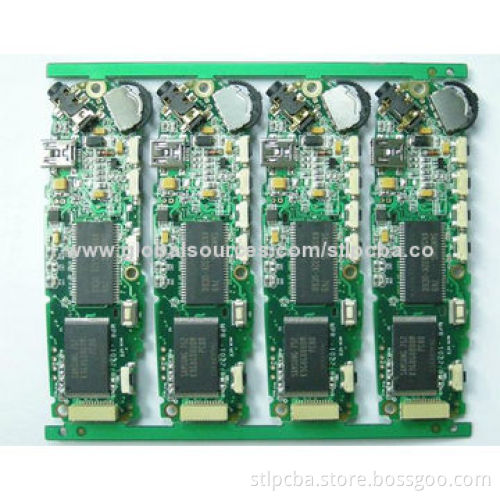
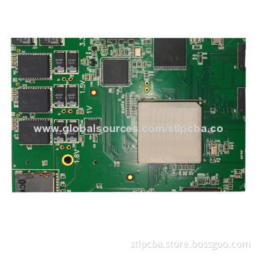
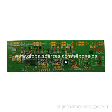
High Density Multilayer PCBs with 550x550mm Maximum Panel Size
- Payment Type:
- T/T in Advance or Western Union
Your message must be between 20 to 2000 characters
Contact Now| Payment Type: | T/T in Advance or Western Union |
|---|
- Number of layers: 4
- Base material: FR4
- Copper thickness: 35/18μm
- Board thickness: 1.6mm (minimum)
- Hole size: 0.25mm (minimum)
- Line width: 0.15mm (minimum)
- Line spacing: 0.15mm
- Surface finish: Immersion Gold
- Color: blue
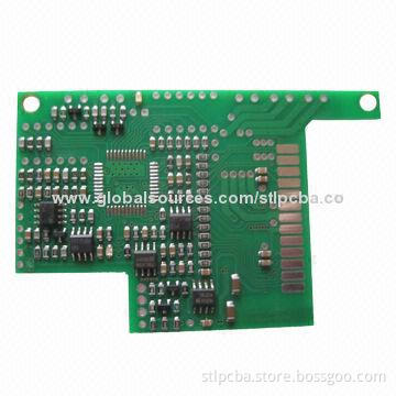
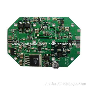
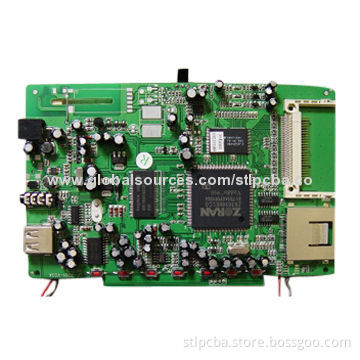
- PCB assembly process: SMT/DIP/assembly
- Packaging detail: carton box with vacuum anti-static bag inner
- Delivery lead time range: 15-20 days
- Gerber file and BOM list
- Clear pictures of PCBA or PCBA sample for us
- Test method for PCBA
Related Keywords
-
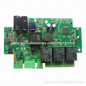
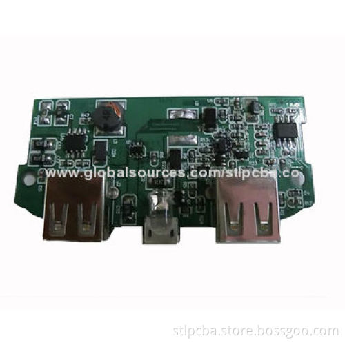
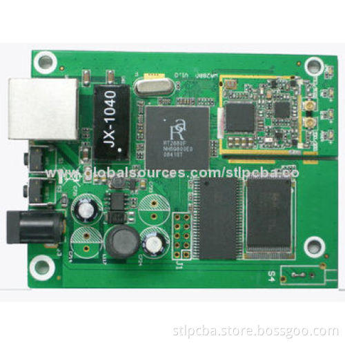
Electronic Assembly, China customized FR4 PCBA, PCB, PCBA OEM & ODM services
SMT Assembly, Manufacturing Circuit, X-Ray for BGA Testing
Contract Manufacturing, one stop PCB assembly with low price
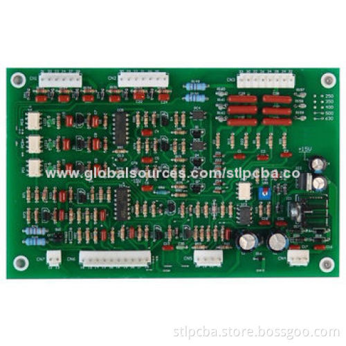
PCB manufacture design, traffic, industrial, sound, home alarm systems
Contract Manufacturing Design, Cost Effective, Production Runs from Small to Large
Related Products-
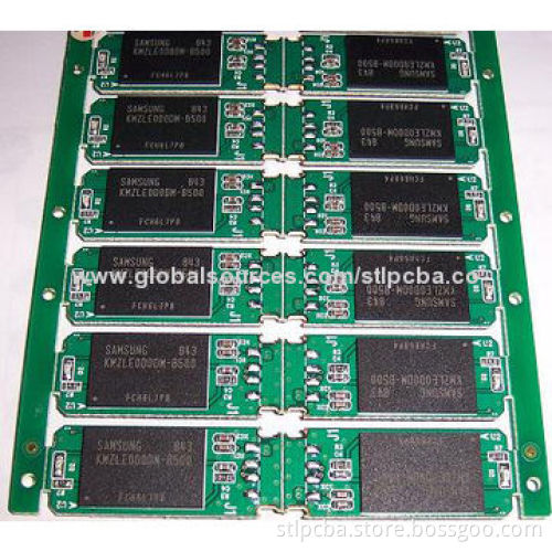
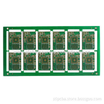
PCB Boards With 4-layer Multilayer, Immersion Gold-plated Surface and 0.25mm Minimum Hole Size
-

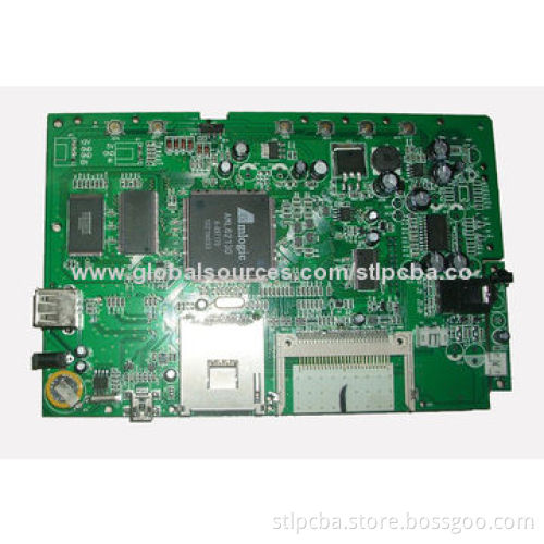
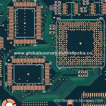
Multi-layered PCBs with Green Solder Mask, Different Surface Finishes are Available
-
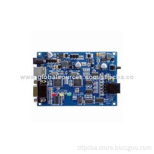
4-layer PCB Board with 2.0mm Thickness, Blind Vias and Immersion Gold
-
Quick Turn High-density Multilayer PCB, FR4 Major Material, Lead-free Surface Finish
-
High Density Multilayer PCBs with 550x550mm Maximum Panel Size
Product Categories-
PCB assemblies(160)
-
FR-4 PCBs(53)
-
Electronic products OEM & ODM services(45)
-
Multilayer PCBs(35)
-
High-density multilayer PCBs(29)
-
Contract manufacturing services(31)
-
Rigid LED strips(28)
-
Aluminum PCBs(17)
-
Single-sided PCBs(12)
-
Double-sided PCBs(10)
-
Copper PCBs(10)
-
Lead free HAL PCBs(4)
-
Flexible PCBs(3)
-
Injection molds(3)
-
Rigid-flex PCBs(2)
-
High frequency PCBs(2)
-
White flexible LED strips(2)
-
Multiple color flexible LED strips(1)