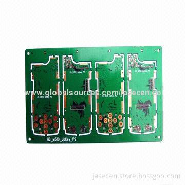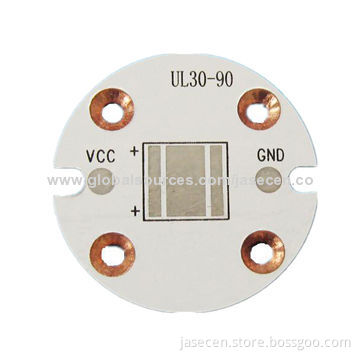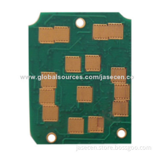
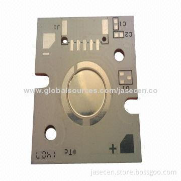
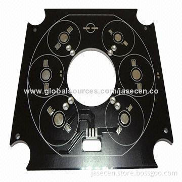
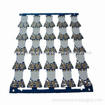
Copper Multilayer PCB
- Payment Type:
- T/T or Western Union
Quantity:
Your message must be between 20 to 2000 characters
Contact NowBasic Info
Basic Info
| Payment Type: | T/T or Western Union |
|---|
Product Description
Product Description
- Layer
- Major material: FR4
- Board thickness: 1.6mm
- Surface finishing: lead free HAL
- Solder mask: green
- Copper thickness: 1oz
- Minimum hole size: 0.3mm
- Minimum line width and spacing: 4-mil
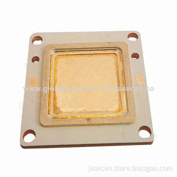
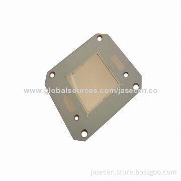
- Materials: FR4/Hi Tg FR4/lead-free (RoHS mark)/CEM-3, aluminum, metal based
- Layers: 1-18
- Finishing board thickness: 0.2-3.5mm (8-138-mil)
- Board thickness tolerance: ±10%
- Copper thickness: 0.5-4oz (18-144um)
- Copper plating hole: 18-40um
- Impedance control: ±10%
- Warp and twist: 0.70%
- Minimum trace width: 0.075mm (3-mil)
- Minimum space width: 0.075mm (3-mil)
- SMD pitch: 0.2mm (8-mil)
- BGA pitch: 0.2mm (8-mil)
- Minimum solder mask dam: 0.0635mm (2.5-mil)
- Solder mask clearance: 0.075mm (3-mil)
- Minimum SMT pad spacing: 0.075mm (3-mil)
- Solder mask thickness: 0.0007-inch (0.018mm)
- Minimum hole size (CNC): 0.2mm (8-mil)
- Minimum punch hole size: 0.9mm (35-mil)
- Hole size tolerance:
- PTH: ±0.075mm
- NPTH: ±0.05mm
- Hole position tolerance: ±0.075mm
Related Keywords
Related Keywords
You May Also Like
You May Also Like
-
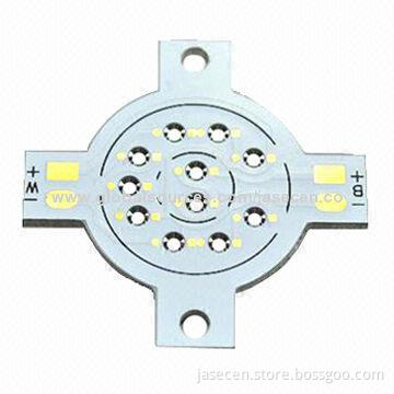
LED PCB with Aluminum Base of 5mm Thickness
Blue Solder Mask Single-sided PCB with Immersion Gold
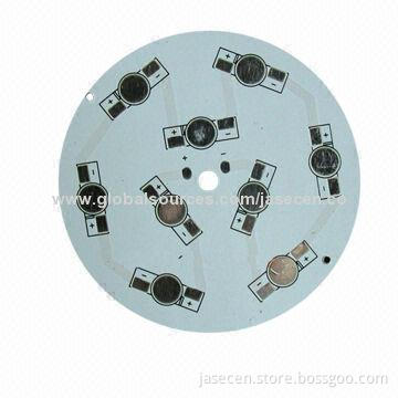
9W Aluminum PCB with thickness of 5.0mm
Related ProductsProduct Categories-
Multilayer PCBs(84)
-
Aluminum PCBs(53)
-
FR-4 PCBs(48)
-
Double-sided PCBs(45)
-
High-density multilayer PCBs(40)
-
Single-sided PCBs(27)
-
Copper PCBs(25)
-
Rigid-flex PCBs(23)
-
Multilayer flexible PCBs(20)
-
Immersion gold PCBs(16)
-
High frequency PCBs(15)
-
PCB assemblies(10)
-
Single-sided flexible PCBs(9)
-
Double-sided flexible PCBs(8)
-
Ceramic PCBs(7)
-
Immersion silver PCBs(5)
-
Lead free HAL PCBs(4)
-
OSP PCBs(3)
-
Impedance control PCBs(2)