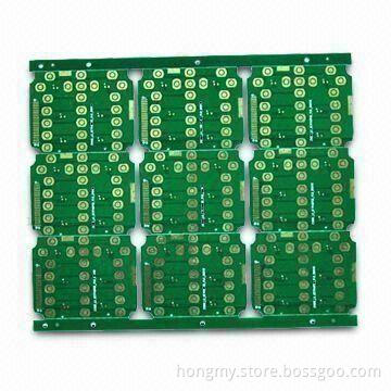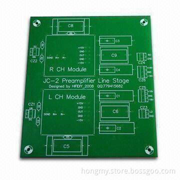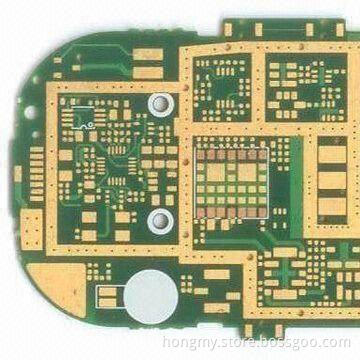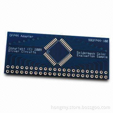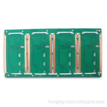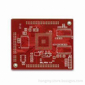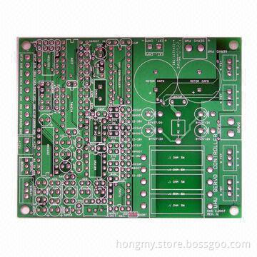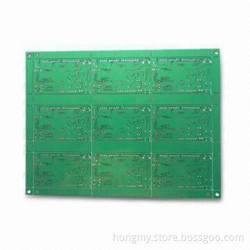
Multilayer PCB with Tg150 Glass Transition, 0.1mm Minimum Line Width and 1oz Copper Thickness
- Payment Type:
- T/T, L/C at Sight, Western Union, PayPal
Quantity:
Your message must be between 20 to 2000 characters
Contact NowBasic Info
Basic Info
| Payment Type: | T/T, L/C at Sight, Western Union, PayPal |
|---|
Product Description
Product Description
- Board thickness: 1.6mm
- Copper thickness: 1oz
- Minimum line width: 0.1mm
- Minimum line spacing: 0.154mm
- Minimum hole diameter: 0.2mm
- Surface finish: immersion gold, (Au 3U inches and 120U inchesNi)
- Solder mask: green
- Glass transition: Tg150
- We offer a wide range of PCBs such as single-sided,double-sided, multi-layer, high-frequency, MCPCB, metal-backed PCBand more
- Our factories got, UL certificates and our products meet RoHSstandards
- RoHS: A001C100827049001-2
- SGS: CANEC1000312001
- UL: E320045
- If our PCBs can meet your requirements, welcomed to receiveyour inquiry or trial order for testing our price and quality
- We will quote to you the best price for your reference as soonas we receive your specific inquiry
- Item manufacture capability
- Materials: FR-4/Hi Tg FR-4/lead-free materials (RoHScompliant)/CEM-3, aluminum, metal based
- Layer number: 1 to 16
- Finished board thickness: 0.2 to 3.8mm (8 to 150mil)
- Board thickness tolerance: ±10%
- Cooper thickness: 0.5 to 6oz (18 to 210 um)
- Copper plating hole: 18 to 40um
- Impedance control: ±10%
- Warp/twist: 0.70%
- Peelable: 0.012 to 0.02 (0.3 to 0.5mm)
- Images:
- Minimum trace width (a): 0.075mm (3mil)
- Minimum space width (b): 0.1mm (4mil)
- Minimum annular ring: 0.1mm (4mil)
- SMD pitch (a): 0.2mm (8mil)
- BGA pitch (b): 0.2mm (8mil), 0.05mm
- Solder mask:
- Minimum solder mask dam (a): 0.0635mm (2.5mil)
- Solder mask clearance (b): 0.1mm (4mil)
- Minimum SMT Pad spacing (c): 0.1mm (4mil)
- Solder mask thickness: 0.0007 inches (0.018mm)
- Minimum trace width (a): 0.075mm (3mil)
- Minimum space width (b): 0.1mm (4mil)
- Minimum annular ring: 0.1mm (4mil)
- SMD pitch (a): 0.2mm (8mil)
- BGA pitch (b): 0.2mm (8mil), 0.05mm
- Minimum solder mask dam (a): 0.0635mm (2.5mil)
- Solder mask clearance (b): 0.1mm (4mil)
- Minimum SMT Pad spacing (c): 0.1mm (4mil)
- Solder mask thickness: 0.0007 inches (0.018mm)
Related Keywords
Related Keywords
You May Also Like
You May Also Like

